SLUS606P June 2004 – November 2015
PRODUCTION DATA.
- 1 Features
- 2 Applications
- 3 Description
- 4 Revision History
- 5 Device Options
- 6 Pin Configuration and Functions
- 7 Specifications
-
8 Detailed Description
- 8.1 Overview
- 8.2 Functional Block Diagram
- 8.3
Feature Description
- 8.3.1 PWM Controller
- 8.3.2 Temperature Qualification
- 8.3.3 Battery Preconditioning (Precharge)
- 8.3.4 Battery Charge Current
- 8.3.5 Battery Voltage Regulation
- 8.3.6 Charge Termination and Recharge
- 8.3.7 Sleep Mode
- 8.3.8 Charge Status Outputs
- 8.3.9 PG Output
- 8.3.10 CE Input (Charge Enable)
- 8.3.11 Timer Fault Recovery
- 8.3.12 Output Overvoltage Protection (Applies to All Versions)
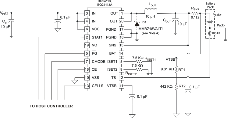
- 8.3.13 Functional Description For System-Controlled Version (bq2411x)
- 8.3.14 Precharge and Fast-Charge Control
- 8.3.15 Charge Termination and Safety Timers
- 8.3.16 Battery Detection
- 8.3.17 Current Sense Amplifier
- 8.4 Device Functional Modes
- 9 Application and Implementation
- 10Power Supply Recommendations
- 11Layout
- 12Device and Documentation Support
- 13Mechanical, Packaging, and Orderable Information
Package Options
Mechanical Data (Package|Pins)
- RHL|20
Thermal pad, mechanical data (Package|Pins)
- RHL|20
Orderable Information
9 Application and Implementation
NOTE
Information in the following applications sections is not part of the TI component specification, and TI does not warrant its accuracy or completeness. TI’s customers are responsible for determining suitability of components for their purposes. Customers should validate and test their design implementation to confirm system functionality.
9.1 Application Information
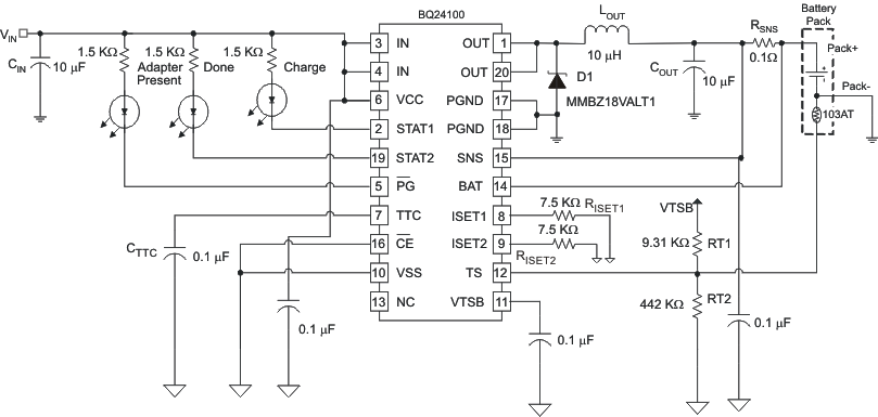
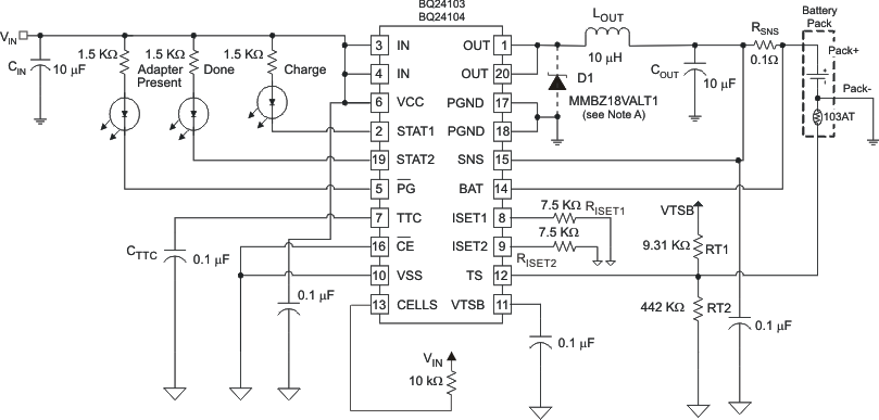
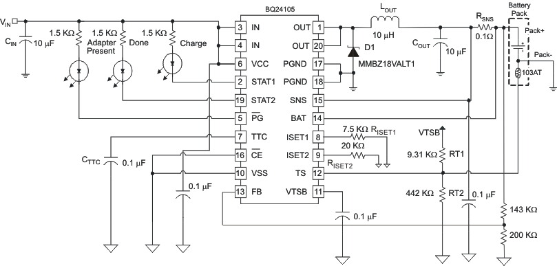
The bqSWITCHER™ battery charger supports precision Li-ion or Li-polymer charging system for single- or two-cell application. The design example below shows the design consideration for a 1-cell application.
9.2 Typical Application
9.2.1 Design Requirements
For this design example, use the parameters listed in Table 3.
Table 3. Design Parameters
| DESIGN PARAMETER | EXAMPLE VALUE |
|---|---|
| AC adapter voltage (VIN) | 16 V |
| Battery charge voltage (number of cells in series) | 4.2 V (1 cell) |
| Battery charge current (during fast charge phase) | 1.33 A |
| Precharge and termination current | 0.133 A |
| Safety timer | 5 hours |
| Inductor ripple current | 30% of fast charge current (0.4 A) |
| Charging temperature range | 0°C to 45°C |
9.2.2 Detailed Design Procedure
- VIN = 16 V
- VBAT = 4.2 V (1-Cell)
- ICHARGE = 1.33 A
- IPRECHARGE = ITERM = 133 mA
- Safety Timer = 5 hours
- Inductor Ripple Current = 30% of Fast Charge Current
- Initiate Charge Temperature = 0°C to 45°C
- Determine the inductor value (LOUT) for the specified charge current ripple:
- Determine the output capacitor value (OUT) using 16 kHz as the resonant frequency:
- Determine the sense resistor using the following equation:
- Determine ISET 1 resistor using the following equation:
- Determine ISET 2 resistor using the following equation:
- Determine TTC capacitor (TTC) for the 5.0 hours safety timer using the following equation:
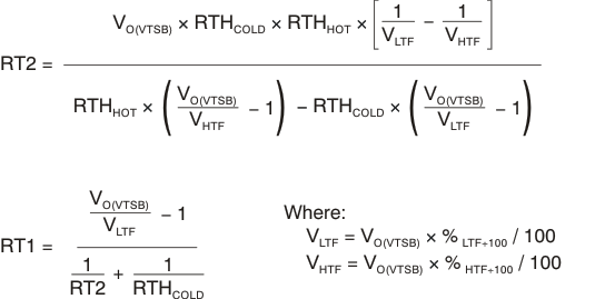
- Determine TS resistor network for an operating temperature range from 0°C to 45°C.
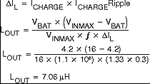
Set the output inductor to standard 10 μH. Calculate the total ripple current with using the 10 μH inductor:

Calculate the maximum output current (peak current):

Use standard 10 μH inductor with a saturation current higher than 1.471 A. (that is, Sumida CDRH74-100)
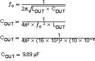
Use standard value 10 μF, 25 V, X5R, ±20% ceramic capacitor (that is, Panasonic 1206 ECJ-3YB1E106M

In order to get better current regulation accuracy (±10%), let VRSNS be between 100 mV and 200 mV. Use VRSNS = 100 mV and calculate the value for the sense resistor.

This value is not standard in resistors. If this happens, then choose the next larger value which in this case is 0.1 Ω. Using the same Equation 15 the actual VRSNS will be 133 mV. Calculate the power dissipation on the sense resistor:

Select standard value 100 mΩ, 0.25 W 0805, 1206 or 2010 size, high precision sensing resistor. (that is., Vishay CRCW1210-0R10F)

Select standard value 7.5 kΩ, 1/16W ±1% resistor (that is, Vishay CRCWD0603-7501-F)

Select standard value 7.5 kΩ, 1/16W ±1% resistor (that is, Vishay CRCWD0603-7501-F)

Select standard value 100 nF, 16V, X7R, ±10% ceramic capacitor (that is, Panasonic ECJ-1VB1C104K). Using this capacitor the actual safety timer will be 4.3 hours.
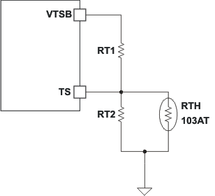 Figure 14. TS Resistor Network
Assuming a 103AT NTC Thermistor on the battery pack, determine the values for RT1 and RT2 using the following equations:

9.2.2.1 Inductor, Capacitor, and Sense Resistor Selection Guidelines
The bqSWITCHER™ provides internal loop compensation. With this scheme, best stability occurs when LC resonant frequency, fo is approximately 16 kHz (8 kHz to 32 kHz). Use Equation 24 to calculate the value of the output inductor and capacitor. Table 4 provides a summary of typical component values for various charge rates.

Table 4. Output Components Summary
| CHARGE CURRENT | 0.5 A | 1 A | 2 A |
|---|---|---|---|
| Output inductor, LOUT | 22 μH | 10 μH | 4.7 μH |
| Output capacitor, COUT | 4.7 μF | 10 μF | 22 μF (or 2 × 10 μF) ceramic |
| Sense resistor, R(SNS) | 0.2 Ω | 0.1 Ω | 0.05 Ω |
9.2.3 Application Curve
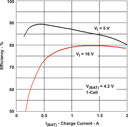 Figure 15. Efficiency vs Charge Current
9.3 System Examples
Figure 19 shows charging a battery and powering system without affecting battery charge and termination.
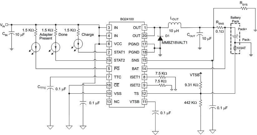 Figure 19. Application Circuit for Charging a Battery and Powering a System
 Without Affecting Termination
The bqSWITCHER™ was designed as a stand-alone battery charger but can be easily adapted to power a system load, while considering a few minor issues.
Advantages:
- The charger controller is based only on what current goes through the current-sense resistor (so precharge, constant current, and termination all work well), and is not affected by the system load.
- The input voltage has been converted to a usable system voltage with good efficiency from the input.
- Extra external FETs are not needed to switch power source to the battery.
- The TTC pin can be grounded to disable termination and keep the converter running and the battery fully charged, or let the switcher terminate when the battery is full and then run off of the battery via the sense resistor.
Other Issues:
- If the system load current is large (≥ 1 A), the IR drop across the battery impedance causes the battery voltage to drop below the refresh threshold and start a new charge. The charger would then terminate due to low charge current. Therefore, the charger would cycle between charging and termination. If the load is smaller, the battery would have to discharge down to the refresh threshold resulting in a much slower cycling. Note that grounding the TTC pin keeps the converter on continuously.
- If TTC is grounded, the battery is kept at 4.2 V (not much different than leaving a fully charged battery set unloaded).
- Efficiency declines 2-3% hit when discharging through the sense resistor to the system.
The following system example shows charging a battery and powering system without affecting battery charge and termination.
The LiFePO4 battery has many unique features such as a high thermal runaway temperature, discharge current capability, and charge current. These special features make it attractive in many applications such as power tools. The recommended charge voltage is 3.6 V and termination current is 50 mA. Figure 20 shows an application circuit for charging one cell LiFePO4 using bq24105. The charge voltage is 3.6 V and recharge voltage is 3.516 V. The fast charging current is set to 1.33 A while the termination current is 50 mA. This circuit can be easily changed to support two or three cell applications. However, only 84 mV difference between regulation set point and rechargeable threshold makes it frequently enter into recharge mode when small load current is applied. This can be solved by lower down the recharge voltage threshold to 200 mV to discharge more energy from the battery before it enters recharge mode again. See the application report, Using the bq24105/25 to Charge LiFePO4 Battery, SLUA443, for additional details. The recharge threshold should be selected according to real application conditions.
