SLUS606P June 2004 – November 2015
PRODUCTION DATA.
- 1 Features
- 2 Applications
- 3 Description
- 4 Revision History
- 5 Device Options
- 6 Pin Configuration and Functions
- 7 Specifications
-
8 Detailed Description
- 8.1 Overview
- 8.2 Functional Block Diagram
- 8.3
Feature Description
- 8.3.1 PWM Controller
- 8.3.2 Temperature Qualification
- 8.3.3 Battery Preconditioning (Precharge)
- 8.3.4 Battery Charge Current
- 8.3.5 Battery Voltage Regulation
- 8.3.6 Charge Termination and Recharge
- 8.3.7 Sleep Mode
- 8.3.8 Charge Status Outputs
- 8.3.9 PG Output
- 8.3.10 CE Input (Charge Enable)
- 8.3.11 Timer Fault Recovery
- 8.3.12 Output Overvoltage Protection (Applies to All Versions)
- 8.3.13 Functional Description For System-Controlled Version (bq2411x)
- 8.3.14 Precharge and Fast-Charge Control
- 8.3.15 Charge Termination and Safety Timers
- 8.3.16 Battery Detection
- 8.3.17 Current Sense Amplifier
- 8.4 Device Functional Modes
- 9 Application and Implementation
- 10Power Supply Recommendations
- 11Layout
- 12Device and Documentation Support
- 13Mechanical, Packaging, and Orderable Information
Package Options
Mechanical Data (Package|Pins)
- RHL|20
Thermal pad, mechanical data (Package|Pins)
- RHL|20
Orderable Information
11 Layout
11.1 Layout Guidelines
It is important to pay special attention to the PCB layout. The following provides some guidelines:
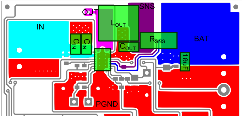
- To obtain optimal performance, the power input capacitors, connected from input to PGND, should be placed as close as possible to the bqSWITCHER™. The output inductor should be placed directly above the IC and the output capacitor connected between the inductor and PGND of the IC. The intent is to minimize the current path loop area from the OUT pin through the LC filter and back to the GND pin. The sense resistor should be adjacent to the junction of the inductor and output capacitor. Route the sense leads connected across the R(SNS) back to the IC, close to each other (minimize loop area) or on top of each other on adjacent layers (do not route the sense leads through a high-current path). Use an optional capacitor downstream from the sense resistor if long (inductive) battery leads are used.
- Place all small-signal components (CTTC, RSET1/2 and TS) close to their respective IC pin (do not place components such that routing interrupts power stage currents). All small control signals should be routed away from the high current paths.
- The PCB should have a ground plane (return) connected directly to the return of all components through vias (3 vias per capacitor for power-stage capacitors, 3 vias for the IC PGND, 1 via per capacitor for small-signal components). A star ground design approach is typically used to keep circuit block currents isolated (high-power/low-power small-signal) which reduces noise-coupling and ground-bounce issues. A single ground plane for this design gives good results. With this small layout and a single ground plane, there is not a ground-bounce issue, and having the components segregated minimizes coupling between signals.
- The high-current charge paths into IN and from the OUT pins must be sized appropriately for the maximum charge current in order to avoid voltage drops in these traces. The PGND pins should be connected to the ground plane to return current through the internal low-side FET. The thermal vias in the IC PowerPAD™ provide the return-path connection.
- The bqSWITCHER™ is packaged in a thermally enhanced MLP package. The package includes a thermal pad to provide an effective thermal contact between the IC and the PCB. Full PCB design guidelines for this package are provided in the application report entitled: QFN/SON PCB Attachment, SLUA271. Six 10-13 mil vias are a minimum number of recommended vias, placed in the IC's power pad, connecting it to a ground thermal plane on the opposite side of the PWB. This plane must be at the same potential as VSS and PGND of this IC.
- See user's guide SLUU200 for an example of a good layout.
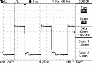
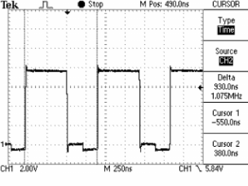
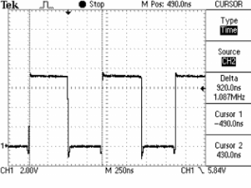
WAVEFORMS: All waveforms are taken at Lout (IC Out pin). VIN = 7.6 V and the battery was set to 2.6 V, 3.5 V, and 4.2 V for the three waveforms. When the top switch of the converter is on, the waveform is at ~7.5 V, and when off, the waveform is near ground. Note that the ringing on the switching edges is small. This is due to a tight layout (minimized loop areas), a shielded inductor (closed core), and using a low-inductive scope ground lead (that is, short with minimum loop).
Precharge: The current is low in precharge; so, the bottom synchronous FET turns off after its minimum on-time which explains the step between ≉0 V and -0.5 V. When the bottom FET and top FET are off, the current conducts through the body diode of the bottom FET which results in a diode drop below the ground potential. The initial negative spike is the delay turning on the bottom FET, which is to prevent shoot-through current as the top FET is turning off.
Fast Charge: This is captured during the constant-current phase. The two negative spikes are the result of the short delay when switching between the top and bottom FETs. The break-before-make action prevents current shoot-through and results in a body diode drop below ground potential during the break time.
Charge during Voltage Regulation and Approaching Termination: Note that this waveform, Figure 23, is similar to the precharge waveform, Figure 21. The difference is that the battery voltage is higher so the duty cycle is slightly higher. The bottom FET stays on longer because there is more of a current load than during precharge; it takes longer for the inductor current to ramp down to the current threshold where the synchronous FET is disabled.
 Figure 21. Precharge Waveform
 Figure 23. Voltage Regulation and Approaching Termination Waveform
 Figure 22. Fast Charge Waveform
11.2 Layout Example
 Figure 24. bq241xx PCB Layout
11.3 Thermal Considerations
The SWITCHER is packaged in a thermally enhanced MLP package. The package includes a thermal pad to provide an effective thermal contact between the IC and the printed circuit board (PCB). Full PCB design guidelines for this package are provided in the application report entitled: QFN/SON PCB Attachment, SLUA271.
The most common measure of package thermal performance is thermal impedance (θJA) measured (or modeled) from the chip junction to the air surrounding the package surface (ambient). The mathematical expression for θJA is:

where
- TJ = chip junction temperature
- TA = ambient temperature
- P = device power dissipation
Factors that can greatly influence the measurement and calculation of θJA include:
- Whether or not the device is board mounted
- Trace size, composition, thickness, and geometry
- Orientation of the device (horizontal or vertical)
- Volume of the ambient air surrounding the device under test and airflow
- Whether other surfaces are in close proximity to the device being tested
The device power dissipation, P, is a function of the charge rate and the voltage drop across the internal power FET. It can be calculated from the following equation:

Due to the charge profile of Li-xx batteries, the maximum power dissipation is typically seen at the beginning of the charge cycle when the battery voltage is at its lowest. (See Figure 3).