SLUS688H March 2006 – November 2015
PRODUCTION DATA.
- 1 Features
- 2 Applications
- 3 Description
- 4 Revision History
- 5 Device Options
- 6 Pin Configuration and Functions
- 7 Specifications
-
8 Detailed Description
- 8.1 Overview
- 8.2 Functional Block Diagram
- 8.3
Feature Description
- 8.3.1 PWM Controller
- 8.3.2 Temperature Qualification
- 8.3.3 Battery Preconditioning (Precharge)
- 8.3.4 Battery Charge Current
- 8.3.5 Battery Voltage Regulation
- 8.3.6 Charge Termination And Recharge
- 8.3.7 Sleep Mode
- 8.3.8 Charge Status Outputs
- 8.3.9 PG Output
- 8.3.10 CE Input (Charge Enable)
- 8.3.11 Timer Fault Recovery
- 8.3.12 Output Overvoltage Protection (Applies to All Versions)
- 8.3.13 Battery Detection
- 8.3.14 Current Sense Amplifier
- 8.4 Device Functional Modes
- 9 Application and Implementation
- 10Power Supply Recommendations
- 11Layout
- 12Device and Documentation Support
- 13Mechanical, Packaging, and Orderable Information
Package Options
Mechanical Data (Package|Pins)
- RHL|20
Thermal pad, mechanical data (Package|Pins)
- RHL|20
Orderable Information
8 Detailed Description
8.1 Overview
The bqSWITCHER supports a precision Li-ion or Li-polymer charging system for single cell or two cell applications. See Figure 16 and Figure 8 for a typical charge profile.
The bq2412X has enhanced EMI performance that helps minimize the number of components needed to meet the FCC-B Standard. The rise time of the OUT pin was slowed down to minimize the radiated EMI.
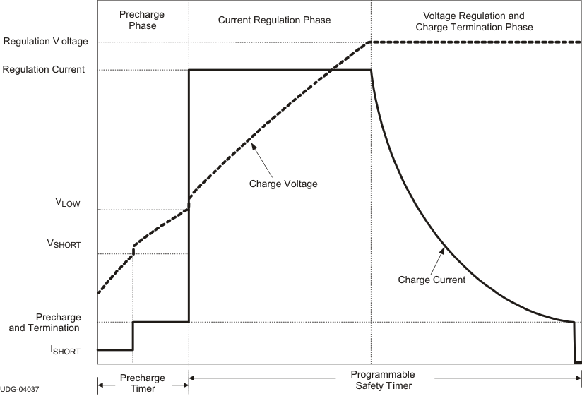 Figure 8. Typical Charging Profile
8.2 Functional Block Diagram
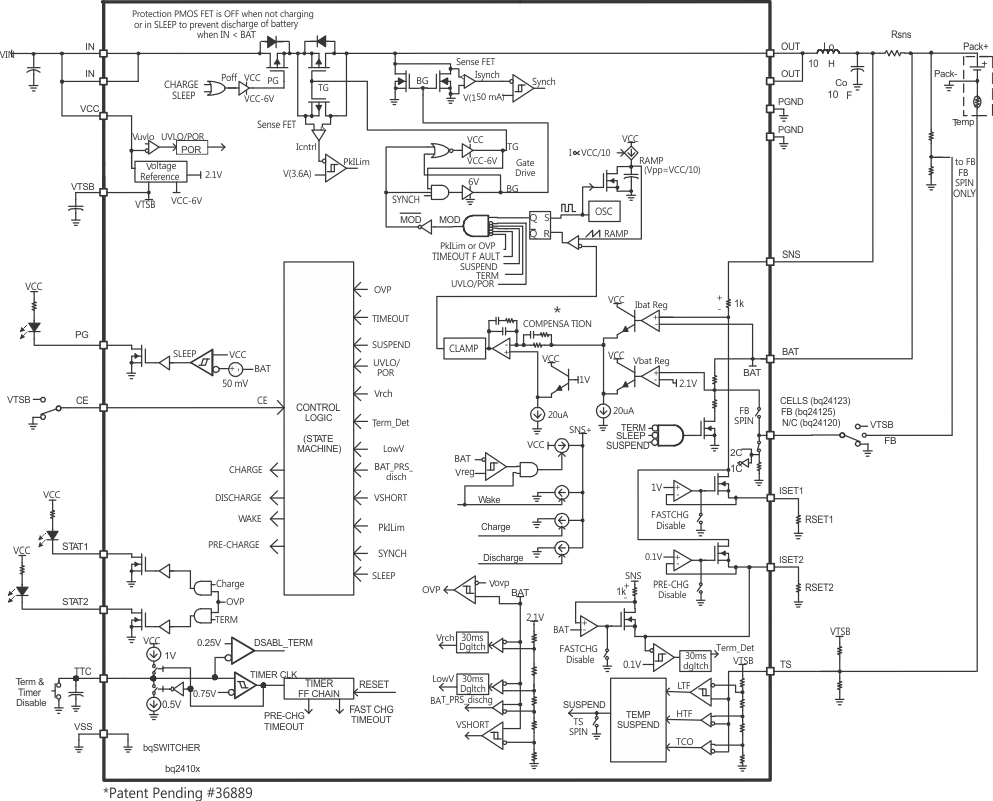
8.3 Feature Description
8.3.1 PWM Controller
The bq2412X provides an integrated fixed 1MHz frequency voltage-mode controller with Feed-Forward function to regulate charge current or voltage. This type of controller is used to help improve line transient response, thereby simplifying the compensation network used for both continuous and discontinuous current conduction operation. The voltage and current loops are internally compensated using a Type-III compensation scheme that provides enough phase boost for stable operation, allowing the use of small ceramic capacitors with very low ESR. There is a 0.5V offset on the bottom of the PWM ramp to allow the device to operate between 0% to 100% duty cycle.
The internal PWM gate drive can directly control the internal PMOS and NMOS power MOSFETs. The high-side gate voltage swings from VCC (when off), to VCC-6 (when on and VCC is greater than 6V) to help reduce the conduction losses of the converter by enhancing the gate an extra volt beyond the standard 5V. The low-side gate voltage swings from 6V, to turn on the NMOS, down to PGND to turn it off. The bq2412X has two back to back common-drain P-MOSFETs on the high side. An input P-MOSFET prevents battery discharge when IN is lower than BAT. The second P-MOSFET behaves as the switching control FET, eliminating the need of a bootstrap capacitor.
Cycle-by-cycle current limit is sensed through the internal high-side sense FET. The threshold is set to a nominal 3.6A peak current. The low-side FET also has a current limit that decides if the PWM Controller will operate in synchronous or non-synchronous mode. This threshold is set to 100mA and it turns off the low-side NMOS before the current reverses, preventing the battery from discharging. Synchronous operation is used when the current of the low-side FET is greater than 100mA to minimize power losses.
8.3.2 Temperature Qualification
The bqSWITCHER continuously monitors battery temperature by measuring the voltage between the TS pin and VSS pin. A negative temperature coefficient thermistor (NTC) and an external voltage divider typically develop this voltage. The bqSWITCHER compares this voltage against its internal thresholds to determine if charging is allowed. To initiate a charge cycle, the battery temperature must be within the V(LTF)-to-V(HTF) thresholds. If battery temperature is outside of this range, the bqSWITCHER suspends charge and waits until the battery temperature is within the V(LTF)-to-V(HTF) range. During the charge cycle (both precharge and fast charge), the battery temperature must be within the V(LTF)-to-V(TCO) thresholds. If battery temperature is outside of this range, the bqSWITCHER suspends charge and waits until the battery temperature is within the V(LTF)-to-V(HTF) range. The bqSWITCHER suspends charge by turning off the PWM and holding the timer value (that is, timers are not reset during a suspend condition). Note that the bias for the external resistor divider is provided from the VTSB output. Applying a constant voltage between the V(LTF)-to-V(HTF) thresholds to the TS pin disables the temperature-sensing feature.
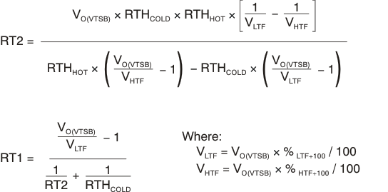
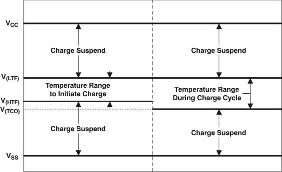 Figure 9. TS Pin Thresholds
8.3.3 Battery Preconditioning (Precharge)
On power up, if the battery voltage is below the VLOWV threshold, the bqSWITCHER applies a precharge current, IPRECHG, to the battery. This feature revives deeply discharged cells. The bqSWITCHER activates a safety timer, tPRECHG, during the conditioning phase. If the VLOWV threshold is not reached within the timer period, the bqSWITCHER turns off the charger and enunciates FAULT on the STATx pins. In the case of a FAULT condition, the bqSWITCHER reduces the current to IDETECT. IDETECT is used to detect a battery replacement condition. Fault condition is cleared by POR or battery replacement.
The magnitude of the precharge current, IO(PRECHG), is determined by the value of programming resistor, R(ISET2), connected to the ISET2 pin.

where
- RSNS is the external current-sense resistor
- V(ISET2) is the output voltage of the ISET2 pin
- K(ISET2) is the V/A gain factor
- V(ISET2) and K(ISET2) are specified in the Electrical Characteristics table.
8.3.4 Battery Charge Current
The battery charge current, IO(CHARGE), is established by setting the external sense resistor, R(SNS), and the resistor, R(ISET1), connected to the ISET1 pin.
In order to set the current, first choose R(SNS) based on the regulation threshold VIREG across this resistor. The best accuracy is achieved whe the VIREG is between 100mV and 200mV.

If the results is not a standard sense resistor value, choose the next larger value. Using the selected standard value, solve for VIREG. Once the sense resistor is selected, the ISET1 resistor can be calculated using the following equation:

8.3.5 Battery Voltage Regulation
The voltage regulation feedback occurs through the BAT pin. This input is tied directly to the positive side of the battery pack. The bqSWITCHER monitors the battery-pack voltage between the BAT and VSS pins. The bqSWITCHER is offered in a fixed single-cell voltage version (4.2 V) and as a one-cell or two-cell version selected by the CELLS input. A low or floating input on the CELLS selects single-cell mode (4.2 V) while a high-input through a resistor selects two-cell mode (8.4 V).
8.3.6 Charge Termination And Recharge
The bqSWITCHER monitors the charging current during the voltage regulation phase. Once the termination threshold, ITERM, is detected, the bqSWITCHER terminates charge. The termination current level is selected by the value of programming resistor, R(ISET2), connected to the ISET2 pin.

where
- R(SNS) is the external current-sense resistor
- VTERM is the output of the ISET2 pin
- K(ISET2) is the A/V gain factor
- VTERM and K(ISET2) are specified in the Electrical Characteristics table
As a safety backup, the bqSWITCHER also provides a programmable charge timer. The charge time is programmed by the value of a capacitor connected between the TTC pin and GND by the following formula:

where
- C(TTC) is the capacitor connected to the TTC pin
- K(TTC) is the multiplier
A new charge cycle is initiated when one of the following conditions is detected:
- The battery voltage falls below the VRCH threshold.
- Power-on reset (POR), if battery voltage is below the VRCH threshold
- CE toggle
- TTC pin, described as follows.
In order to disable the charge termination and safety timer, the user can pull the TTC input below the VTTC_EN threshold. Going above this threshold enables the termination and safety timer features and also resets the timer. Tying TTC high disables the safety timer only.
8.3.7 Sleep Mode
The bqSWITCHER enters the low-power sleep mode if the VCC pin is removed from the circuit. This feature prevents draining the battery during the absence of VCC.
8.3.8 Charge Status Outputs
The open-drain STAT1 and STAT2 outputs indicate various charger operations as shown in Table 1. These status pins can be used to drive LEDs or communicate to the host processor. Note that OFF indicates that the open-drain transistor is turned off.
Table 1. Status Pins Summary
| CHARGE STATE | STAT1 | STAT2 |
|---|---|---|
| Charge-in-progress | ON | OFF |
| Charge complete | OFF | ON |
| Charge suspend, timer fault, overvoltage, sleep mode, battery absent | OFF | OFF |
8.3.9 PG Output
The open-drain PG (power good) indicates when the AC-to-DC adapter (that is, VCC) is present. The output turns on when sleep-mode exit threshold, VSLP-EXIT, is detected. This output is turned off in the sleep mode. The PG pin can be used to drive an LED or communicate to the host processor.
8.3.10 CE Input (Charge Enable)
The CE digital input is used to disable or enable the charge process. A low-level signal on this pin enables the charge and a high-level VCC signal disables the charge. A high-to-low transition on this pin also resets all timers and fault conditions. Note that the CE pin should not be tied to VTSB. This may create power-up issues.
8.3.11 Timer Fault Recovery
As shown in Figure 16, bqSWITCHER provides a recovery method to deal with timer fault conditions. The following summarizes this method.
Condition 1 VI(BAT) above recharge threshold (VOREG - VRCH) and timeout fault occurs.
Recovery method: bqSWITCHER waits for the battery voltage to fall below the recharge threshold. This could happen as a result of a load on the battery, self-discharge or battery removal. Once the battery falls below the recharge threshold, the bqSWITCHER clears the fault and enters the battery absent detection routine. A POR or CE toggle also clears the fault.
Condition 2 Charge voltage below recharge threshold (VOREG – VRCH) and timeout fault occurs
Recovery method: Under this scenario, the bqSWITCHER applies the IDETECT current. This small current is used to detect a battery removal condition and remains on as long as the battery voltage stays below the recharge threshold. If the battery voltage goes above the recharge threshold, then the bqSWITCHER disables the IDETECT current and executes the recovery method described in Condition 1. Once the battery falls below the recharge threshold, the bqSWITCHER clears the fault and enters the battery absent detection routine. A POR or CE toggle also clears the fault.
8.3.12 Output Overvoltage Protection (Applies to All Versions)
The bqSWITCHER provides a built-in overvoltage protection to protect the device and other components against damages if the battery voltage gets too high, as when the battery is suddenly removed. When an overvoltage condition is detected, this feature turns off the PWM and STATx pins. The fault is cleared once VIBAT drops to the recharge threshold (VOREG - VRCH).
8.3.13 Battery Detection
For applications with removable battery packs, bqSWITCHER provides a battery absent detection scheme to reliably detect insertion and/or removal of battery packs.
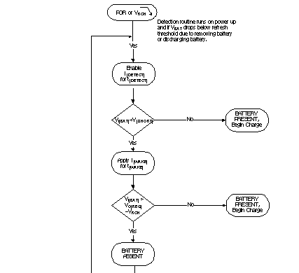 Figure 10. Battery Detection for bq2412x ICs
The voltage at the BAT pin is held above the battery recharge threshold, VOREG – VRCH, by the charged battery following fast charging. When the voltage at the BAT pin falls to the recharge threshold, either by a load on the battery or due to battery removal, the bqSWITCHER begins a battery absent detection test. This test involves enabling a detection current, IDISCHARGE1, for a period of tDISCHARGE1 and checking to see if the battery voltage is below the short circuit threshold, VSHORT. Following this, the wake current, IWAKE is applied for a period of tWAKE and the battery voltage is checked again to ensure that it is above the recharge threshold. The purpose of this current is to attempt to close an open battery pack protector, if one is connected to the bqSWITCHER.
Passing both of the discharge and charge tests indicates a battery absent fault at the STAT pins. Failure of either test starts a new charge cycle. For the absent battery condition, typically the voltage on the BAT pin rises and falls between 0V and VOVP thresholds indefinitely.
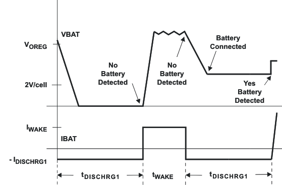 Figure 11. Battery Detect Timing Diagram
8.3.13.1 Battery Detection Example
In order to detect a no battery condition during the discharge and wake tests, the maximum output capacitance should not exceed the following:
- Discharge (IDISCHRG1 = 400 μA, tDISCHRG1 = 1s, VSHORT = 2V)
- Wake (IWAKE = 2 mA, tWAKE = 0.5 s, VOREG – VRCH = 4.1V)
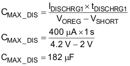
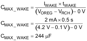
Based on these calculations the recommended maximum output capacitance to ensure proper operation of the battery detection scheme is 100 μF which will allow for process and temperature variations.
Figure 12 shows the battery detection scheme when a battery is inserted. Channel 3 is the output signal and Channel 4 is the output current. The output signal switches between VOREG and GND until a battery is inserted. Once the battery is detected, the output current increases from 0A to 1.3A, which is the programmed charge current for this application.
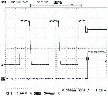 Figure 12. Battery Detection Waveform When a Battery is Inserted
Figure 13 shows the Battery Detection scheme when a battery is removed. Channel 3 is the output signal and Channel 4 is the output current. When the battery is removed, the output signal goes up due to the stored energy in the inductor and it crosses the VOREG – VRCH threshold. At this point the output current goes to 0A and the IC terminates the charge process and turns on the IDISCHG2 for tDISCHG2. This causes the output voltage to fall down below the VOREG – VRCHG threshold triggering a Battery Absent condition and starting the Battery Detection scheme.
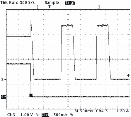 Figure 13. Battery Detection Waveform When a Battery is Removed
8.3.14 Current Sense Amplifier
BQ2412X family offers a current sense amplifier feature that translates the charge current into a DC voltage. Figure 14 is a block diagram of this feature.
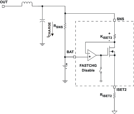 Figure 14. Current Sense Amplifier
The voltage on the ISET2 pin can be used to calculate the charge current. Equation 9 shows the relationship between the ISET2 voltage and the charge current:

This feature can be used to monitor the charge current during the current regulation phase (Fastcharge only) and the voltage regulation phase. The schematics for the application circuit for this waveform is shown in Figure 21
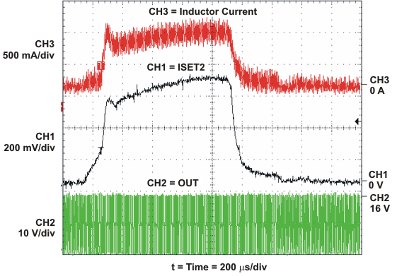 Figure 15. Current Sense Amplifier
8.4 Device Functional Modes
Figure 16 shows the operational flow chart for a typical charge operation.
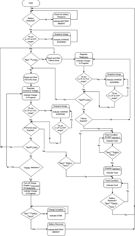 Figure 16. Operational Flow Chart