SLUSAB0D October 2010 – April 2016
UNLESS OTHERWISE NOTED, this document contains PRODUCTION DATA.
- 1 Features
- 2 Applications
- 3 Description
- 4 Revision History
- 5 Description (Continued)
- 6 Device Comparisons
- 7 Pin Configuration and Functions
- 8 Specifications
-
9 Detailed Description
- 9.1 Overview
- 9.2 Functional Block Diagram
- 9.3 Feature Description
- 9.4
Device Functional Modes
- 9.4.1 Charge Mode Operation
- 9.4.2 PWM Controller in Charge Mode
- 9.4.3 Battery Charging Process
- 9.4.4 Thermal Regulation and Protection
- 9.4.5 Charge Status Output, STAT Pin
- 9.4.6 Control Bits in Charge Mode
- 9.4.7 Control Pins in Charge Mode
- 9.4.8 BOOST Mode Operation (bq24153A/8 only)
- 9.4.9 High Impedance (HI-Z) Mode
- 9.5 Programming
- 9.6
Register Maps
- 9.6.1 Status/Control Register [Memory Location: 00, Reset State: x1xx 0xxx]
- 9.6.2 Control Register [Memory Location: 01, Reset State: 0011 0000]
- 9.6.3 Control/Battery Voltage Register [Memory Location: 02, Reset State: 0000 1010]
- 9.6.4 Vender/Part/Revision Register [Memory Location: 03, Reset State: 0101 000x]
- 9.6.5 Battery Termination/Fast Charge Current Register [Memory Location: 04, Reset State: 0000 000]
- 9.6.6 Special Charger Voltage/Enable Pin Status Register [Memory location: 05, Reset state: 001X X100]
- 9.6.7 Safety Limit Register [Memory location: 06, Reset state: 01000000]
- 10Application and Implementation
- 11Power Supply Recommendations
- 12Layout
- 13Device and Documentation Support
- 14Mechanical, Packaging, and Orderable Information
Package Options
Mechanical Data (Package|Pins)
- YFF|20
Thermal pad, mechanical data (Package|Pins)
Orderable Information
1 Features
- Charge Faster than Linear Chargers
- High-Accuracy Voltage and Current Regulation
- Input Current Regulation Accuracy: ±5% (100 mA and 500 mA)
- Charge Voltage Regulation Accuracy: ±0.5% (25°C), ±1% (0°C to 125°C)
- Charge Current Regulation Accuracy: ±5%
- Input Voltage Based Dynamic Power Management (VIN DPM)
- Bad Adaptor Detection and Rejection
- Safety Limit Register for Maximum Charge Voltage and Current Limiting
- High-Efficiency Mini-USB/AC Battery Charger for Single-Cell Li-Ion and Li-Polymer Battery Packs
- 20-V Absolute Maximum Input Voltage Rating
- 9-V Maximum Operating Input Voltage-bq24156A/9
- 6-V Maximum Operating Input Voltage-bq24153A/8
- Built-In Input Current Sensing and Limiting
- Integrated Power FETs for Up To 1.55-A Charge Rate
- Programmable Charge Parameters through I2C™ Compatible Interface (up to 3.4 Mbps):
- Input Current Limit
- VIN DPM Threshold
- Fast-Charge/Termination Current
- Charge Regulation Voltage (3.5 V to 4.44 V)
- Low Charge Current Mode Enable/Disable
- Safety Timer with Reset Control
- Termination Enable/Disable
- Support up to 1.55 A Charge Current Using 55-mΩ Sensing Resistor
- Synchronous Fixed-Frequency PWM Controller Operating at 3 MHz With 0% to 99.5% Duty Cycle
- Automatic High Impedance Mode for Low Power Consumption
- Robust Protection
- Reverse Leakage Protection Prevents Battery Drainage
- Thermal Regulation and Protection
- Input/Output Overvoltage Protection
- Status Output for Charging and Faults
- USB Friendly Boot-Up Sequence
- Automatic Charging
- Power Up System without Battery bq24158/9
- Boost Mode Operation for USB OTG: (bq24153A/8 only)
- Input Voltage Range (from Battery): 2.5 V to 4.5 V
- Output for VBUS: 5.05 V/ 200 mA
- 2.1 mm x 2 mm 20-Pin WCSP Package
2 Applications
- Mobile and Smart Phones
- MP3 Players
- Handheld Devices
3 Description
The bq24153A/6A/8/9 is a compact, flexible, high-efficiency, USB-friendly switch-mode charge management device for single-cell Li-ion and Li-polymer batteries used in a wide range of portable applications. The charge parameters can be programmed through an I2C interface. The IC integrates a synchronous PWM controller, power MOSFETs, input current sensing, high-accuracy current and voltage regulation, and charge termination, into a small WCSP package.
Device Information(1)
| PART NUMBER | PACKAGE | BODY SIZE (NOM) |
|---|---|---|
| bq24153A, bq24156A, bq24158, bq24159 |
20-Pin WCSP | 2.1 mm x 2 mm |
- For all available packages, see the orderable addendum at the end of the datasheet.
4 Revision History
Changes from C Revision (July 2013) to D Revision
- Added the Device Information table, ESD Ratings table, Detailed Description section, Application and Implementation section, Power Supply Recommendation section, Layout section, Device and Documentation Support section, and the Mechanical, Packaging, and Orderable Information sectionGo
- Changed Features bullet From: "...1.5-A Charge Rate" To: "...1.55-A Charge Rate"Go
- Added Features bullet: "Support up to 1.55A......Sensing Resistor "Go
- Added information to the Device Comparisons table.Go
- Changed t32S in the Timing Requirements table, PROTECTION section, MAX value From: 32s To 40s Go
- Added information to bullet note at Table 9 for clarification. Go
Changes from B Revision (August 2012) to C Revision
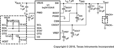
- Changed Boot capacitor value from 10 nF to 33 nF in Typical Application CircuitGo
- Changed BOOT capacitor value from 10 nF to 33 nF in Pin Functions DescriptionGo
- Changed CBOOT capacitor value from 10 nF to 33 nF in Figure 25 and Figure 36 Go
Changes from A Revision (February 2012) to B Revision
- Changed the revision to Rev B, August 2012Go
- Deleted the last sentence in the PIN Functions table: Name CD, in the description columnGo
- Changed IO(CHARGE) Test Conditions statement from "V(LOWV)" to "V(SHORT)"Go
- Deleted from the CD Pin (Charge Disable) section the last sentence: In 15-minute....32-second timer.Go
Changes from * Revision (October 2010) to A Revision
- Added bq24159 throughout this data sheet.Go
- Changed the Device Comparisons tableGo
