SLUSAB0D October 2010 – April 2016
UNLESS OTHERWISE NOTED, this document contains PRODUCTION DATA.
- 1 Features
- 2 Applications
- 3 Description
- 4 Revision History
- 5 Description (Continued)
- 6 Device Comparisons
- 7 Pin Configuration and Functions
- 8 Specifications
-
9 Detailed Description
- 9.1 Overview
- 9.2 Functional Block Diagram
- 9.3 Feature Description
- 9.4
Device Functional Modes
- 9.4.1 Charge Mode Operation
- 9.4.2 PWM Controller in Charge Mode
- 9.4.3 Battery Charging Process
- 9.4.4 Thermal Regulation and Protection
- 9.4.5 Charge Status Output, STAT Pin
- 9.4.6 Control Bits in Charge Mode
- 9.4.7 Control Pins in Charge Mode
- 9.4.8 BOOST Mode Operation (bq24153A/8 only)
- 9.4.9 High Impedance (HI-Z) Mode
- 9.5 Programming
- 9.6
Register Maps
- 9.6.1 Status/Control Register [Memory Location: 00, Reset State: x1xx 0xxx]
- 9.6.2 Control Register [Memory Location: 01, Reset State: 0011 0000]
- 9.6.3 Control/Battery Voltage Register [Memory Location: 02, Reset State: 0000 1010]
- 9.6.4 Vender/Part/Revision Register [Memory Location: 03, Reset State: 0101 000x]
- 9.6.5 Battery Termination/Fast Charge Current Register [Memory Location: 04, Reset State: 0000 000]
- 9.6.6 Special Charger Voltage/Enable Pin Status Register [Memory location: 05, Reset state: 001X X100]
- 9.6.7 Safety Limit Register [Memory location: 06, Reset state: 01000000]
- 10Application and Implementation
- 11Power Supply Recommendations
- 12Layout
- 13Device and Documentation Support
- 14Mechanical, Packaging, and Orderable Information
Package Options
Mechanical Data (Package|Pins)
- YFF|20
Thermal pad, mechanical data (Package|Pins)
Orderable Information
8 Specifications
8.1 Absolute Maximum Ratings(1) (2)
over operating free-air temperature range (unless otherwise noted)| bq24153A/6A/8/9 | UNIT | ||||
|---|---|---|---|---|---|
| MIN | MAX | ||||
| Supply voltage (with respect to PGND(3)) | VBUS; VPMID ≥ VBUS –0.3 V | –2 | 20 | V | |
| Input voltage (with respect to PGND(3)) | SCL, SDA, OTG, SLRST, CSIN, CSOUT, CD | –0.3 | 7 | V | |
| Output voltage (with respect to PGND(3)) | PMID, STAT | –0.3 | 20 | V | |
| VREF | 7 | V | |||
| SW, BOOT | –0.7 | 20 | V | ||
| Voltage difference between CSIN and CSOUT inputs (V(CSIN) – V(CSOUT) ) | –7 | 7 | V | ||
| Voltage difference between BOOT and SW inputs (V(BOOT) – V(SW) ) | –0.3 | 7 | V | ||
| Voltage difference between VBUS and PMID inputs (V(VBUS) – V(PMID) ) | –7 | 0.7 | V | ||
| Voltage difference between PMID and SW inputs (V(PMID) – V(SW) ) | –0.7 | 20 | V | ||
| Output sink | STAT | 10 | mA | ||
| Output Current (average) | SW | 1.55(2) | A | ||
| TA | Operating free-air temperature range | –30 | 85 | °C | |
| TJ | Junction temperature | –40 | 125 | °C | |
| Tstg | Storage temperature | –45 | 150 | °C | |
(1) Stresses beyond those listed under absolute maximum ratings may cause permanent damage to the device. These are stress ratings only, and functional operation of the device at these or any other conditions beyond those indicated under recommended operating conditions is not implied. Exposure to absolute-maximum-rated conditions for extended periods may affect device reliability. All voltage values are with respect to the network ground terminal unless otherwise noted.
(2) Duty cycle for output current should be less than 50% for 10- year life time when output current is above 1.25A.
(3) All voltages are with respect to PGND if not specified. Currents are positive into, negative out of the specified terminal, if not specified. Consult Packaging Section of the data sheet for thermal limitations and considerations of packages.
8.2 ESD Ratings
| VALUE | UNIT | |||
|---|---|---|---|---|
| V(ESD) | Electrostatic discharge | Human body model (HBM), per ANSI/ESDA/JEDEC JS-001, all pins(1) | ±2000 | V |
| Charged device model (CDM), per JEDEC specification JESD22-C101, all pins(2) | ±500 | |||
(1) JEDEC document JEP155 states that 500-V HBM allows safe manufacturing with a standard ESD control process.
(2) JEDEC document JEP157 states that 250-V CDM allows safe manufacturing with a standard ESD control process.
8.3 Recommended Operating Conditions
| MIN | NOM | MAX | UNIT | ||
|---|---|---|---|---|---|
| VBUS | Supply voltage, bq24153A/8 | 4 | 6(1) | V | |
| VBUS | Supply voltage, bq24156A/9 | 4 | 9(1) | V | |
| TJ | Operating junction temperature range | –40 | 125 | °C |
(1) The inherent switching noise voltage spikes should not exceed the absolute maximum rating on either the BOOST or SW pins. A tight layout minimizes switching noise.
8.4 Thermal Information
| THERMAL METRIC(1) | bq24153A/6A/8/9 | UNIT | |
|---|---|---|---|
| YFF (DSBGA) | |||
| 20 Pins | |||
| RθJA | Junction-to-ambient thermal resistance | 85 | °C/W |
| RθJC(top) | Junction-to-case (top) thermal resistance | 25 | °C/W |
| RθJB | Junction-to-board thermal resistance | 55 | °C/W |
| ψJT | Junction-to-top characterization parameter | 4 | °C/W |
| ψJB | Junction-to-board characterization parameter | 50 | °C/W |
| RθJC(bot) | Junction-to-case (bottom) thermal resistance | n/a | °C/W |
(1) For more information about traditional and new thermal metrics, see the Semiconductor and IC Package Thermal Metrics application report, SPRA953.
8.5 Electrical Characteristics
Circuit of Figure 25, VBUS = 5 V, HZ_MODE = 0, OPA_MODE = 0 (CD = 0), TJ = –40°C to 125°C, TJ = 25°C for typical values (unless otherwise noted)| PARAMETER | TEST CONDITIONS | MIN | TYP | MAX | UNIT | ||
|---|---|---|---|---|---|---|---|
| INPUT CURRENTS | |||||||
| I(VBUS) | VBUS supply current control | VBUS > VBUS(min), PWM switching | 10 | mA | |||
| VBUS > VBUS(min), PWM NOT switching | 5 | ||||||
| 0°C < TJ < 85°C, CD=1 or HZ_MODE=1 | 15 | 23 | μA | ||||
| Ilgk | Leakage current from battery to VBUS pin | 0°C < TJ < 85°C, V(CSOUT) = 4.2 V, High Impedance mode, VBUS = 0 V | 5 | μA | |||
| Battery discharge current in High Impedance mode, (CSIN, CSOUT, SW pins) | 0°C < TJ < 85°C, V(CSOUT) = 4.2 V, High Impedance mode, V = 0 V, SCL, SDA, OTG = 0 V or 1.8 V |
23 | μA | ||||
| VOLTAGE REGULATION | |||||||
| V(OREG) | Output regulation voltage programable range | Operating in voltage regulation, programmable | 3.5 | 4.44 | V | ||
| Voltage regulation accuracy | TA = 25°C | –0.5% | 0.5% | ||||
| –1% | 1% | ||||||
| CURRENT REGULATION (FAST CHARGE) | |||||||
| IO(CHARGE) | Output charge current programmable range | bq24153A/8, V(SHORT) ≤ V(CSOUT) < V(OREG), VBUS > V(SLP), R(SNS) = 68 mΩ, LOW_CHG=0, Programmable |
550 | 1250 | mA | ||
| bq24156A/9, V(SHORT) ≤ V(CSOUT) < V(OREG), VBUS > V(SLP), R(SNS) = 68 mΩ, LOW_CHG=0, Programmable |
550 | 1550 | mA | ||||
| Low charge current (default after POR in 15 min mode) for bq24153A/6A/8/9 | VSHORT ≤ VCSOUT < VOREG, VBUS >VSLP, RSNS= 68 mΩ, LOW_CHG=1, OTG=High for bq24153A/8 |
325 | 350 | mA | |||
| Regulation accuracy of the voltage across R(SNS) (for charge current regulation)
V(IREG) = IO(CHARGE) × R(SNS) |
37.4 mV ≤ V(IREG)< 44.2mV | –3.5% | 3.5% | ||||
| 44.2 mV ≤ V(IREG) | –3% | 3% | |||||
| WEAK BATTERY DETECTION | |||||||
| V(LOWV) | Weak battery voltage threshold programmable range2 (2) | Adjustable using I2C control | 3.4 | 3.7 | V | ||
| Weak battery voltage accuracy | –5% | 5% | |||||
| Hysteresis for V(LOWV) | Battery voltage falling | 100 | mV | ||||
| CD, OTG and SLRST PIN LOGIC LEVEL | |||||||
| VIL | Input low threshold level | 0.4 | V | ||||
| VIH | Input high threshold level | 1.3 | V | ||||
| I(bias) | Input bias current | Voltage on control pin is 5 V | 1.0 | µA | |||
| CHARGE TERMINATION DETECTION | |||||||
| I(TERM) | Termination charge current programmable range | V(CSOUT) > V(OREG) – V(RCH), VBUS > V(SLP), R(SNS) = 68 mΩ, Programmable |
50 | 400 | mA | ||
| Regulation accuracy for termination current across R(SNS)
V(IREG_TERM) = IO(TERM) × R(SNS) |
3.4 mV ≤ V(IREG_TERM) ≤ 6.8 mV | –15% | 15% | ||||
| 6.8 mV < V(IREG_TERM) ≤ 17 mV | –10% | 10% | |||||
| 17 mV < V(IREG_TERM) ≤ 27.2 mV | –5.5% | 5.5% | |||||
| BAD ADAPTOR DETECTION | |||||||
| VIN(min) | Input voltage lower limit | BAD ADAPTOR DETECTION | 3.6 | 3.8 | 4.0 | V | |
| Hysteresis for VIN(min) | Input voltage rising | 100 | 200 | mV | |||
| ISHORT | Current source to GND | During bad adaptor detection | 20 | 30 | 40 | mA | |
| INPUT BASED DYNAMIC POWER MANAGEMENT | |||||||
| VIN_DPM | Input Voltage DPM threshold programmable range | 4.2 | 4.76 | V | |||
| VIN DPM threshold accuracy | –3% | 1% | |||||
| INPUT CURRENT LIMITING | |||||||
| IIN_LIMIT | Input current limiting threshold | IIN = 100 mA | TJ = 0°C – 125°C | 88 | 93 | 98 | mA |
| TJ = –40°C –125°C | 86 | 93 | 98 | ||||
| IIN = 500 mA | TJ = 0°C – 125°C | 450 | 475 | 500 | mA | ||
| TJ = –40°C –125°C | 440 | 475 | 500 | ||||
| VREF BIAS REGULATOR | |||||||
| VREF | Internal bias regulator voltage | VBUS >VIN(min) or V(CSOUT) > VBUS(min), I(VREF) = 1 mA, C(VREF) = 1 μF |
2 | 6.5 | V | ||
| VREF output short current limit | 30 | mA | |||||
| BATTERY RECHARGE THRESHOLD | |||||||
| V(RCH) | Recharge threshold voltage | Below V(OREG) | 100 | 120 | 150 | mV | |
| STAT OUTPUTS | |||||||
| VOL(STAT) | Low-level output saturation voltage, STAT pin | IO = 10 mA, sink current | 0.55 | V | |||
| High-level leakage current for STAT | Voltage on STAT pin is 5 V | 1 | μA | ||||
| I2C BUS LOGIC LEVELS AND TIMING CHARACTERISTICS | |||||||
| VOL | Output low threshold level | IO = 10 mA, sink current | 0.4 | V | |||
| VIL | Input low threshold level | V(pull-up) = 1.8 V, SDA and SCL | 0.4 | V | |||
| VIH | Input high threshold level | V(pull-up) = 1.8 V, SDA and SCL | 1.2 | V | |||
| I(BIAS) | Input bias current | V(pull-up) = 1.8 V, SDA and SCL | 1 | μA | |||
| f(SCL) | SCL clock frequency | 3.4 | MHz | ||||
| BATTERY DETECTION | |||||||
| I(DETECT) | Battery detection current before charge done (sink current) (1) | Begins after termination detected, V(CSOUT) ≤ V(OREG) |
–0.5 | mA | |||
| SLEEP COMPARATOR | |||||||
| V(SLP) | Sleep-mode entry threshold, VBUS – VCSOUT |
2.3 V ≤ V(CSOUT) ≤ V(OREG), VBUS falling | 0 | 40 | 100 | mV | |
| V(SLP_EXIT) | Sleep-mode exit hysteresis | 2.3 V ≤ V(CSOUT) ≤ V(OREG) | 140 | 200 | 260 | mV | |
| UNDERVOLTAGE LOCKOUT (UVLO) | |||||||
| UVLO | IC active threshold voltage | VBUS rising - Exits UVLO | 3.05 | 3.3 | 3.55 | V | |
| UVLO(HYS) | IC active hysteresis | VBUS falling below UVLO - Enters UVLO | 120 | 150 | mV | ||
| PWM | |||||||
| Voltage from BOOT pin to SW pin | During charge or boost operation | 6.5 | V | ||||
| Internal top reverse blocking MOSFET on-resistance | IIN(LIMIT) = 500 mA, Measured from VBUS to PMID | 180 | 250 | mΩ | |||
| Internal top N-channel Switching MOSFET on-resistance | Measured from PMID to SW, VBOOT – VSW= 4V |
120 | 250 | ||||
| Internal bottom N-channel MOSFET on-resistance | Measured from SW to PGND | 110 | 210 | ||||
| f(OSC) | Oscillator frequency | 3.0 | MHz | ||||
| Frequency accuracy | –10% | 10% | |||||
| D(MAX) | Maximum duty cycle | 99.5% | |||||
| D(MIN) | Minimum duty cycle | 0 | |||||
| Synchronous mode to non-synchronous mode transition current threshold(1) | Low-side MOSFET cycle-by-cycle current sensing | 100 | mA | ||||
| CHARGE MODE PROTECTION | |||||||
| VOVP_IN_USB | Input VBUS OVP threshold voltage (bq24153A/8) | VBUS threshold to turn off converter during charge | 6.3 | 6.5 | 6.7 | V | |
| V(OVP_IN_USB) hysteresis (bq24153A/8) | VBUS falling from above V(OVP_IN_USB) | 170 | mV | ||||
| VOVP-IN_DYN | Input VBUS OVP threshold voltage (bq24156A) | Threshold over VBUS to turn off converter during charge | 9.57 | 9.8 | 10 | ||
| V(OVP_IN_DYN) hysteresis (bq24156A/9) | VBUS falling from above V(OVP_IN_DYN) | 140 | |||||
| VOVP | Output OVP threshold voltage | V(CSOUT) threshold over V(OREG) to turn off charger during charge | 110 | 117 | 121 | %V OREG | |
| V(OVP) hysteresis | Lower limit for V(CSOUT) falling from above V(OVP) | 11 | |||||
| ILIMIT | Cycle-by-cycle current limit for charge | Charge mode operation | 1.8 | 2.4 | 3.0 | A | |
| VSHORT | Trickle to fast charge threshold | V(CSOUT) rising | 2.0 | 2.1 | 2.2 | V | |
| VSHORT hysteresis | V(CSOUT) falling below VSHORT | 100 | mV | ||||
| ISHORT | Trickle charge charging current | V(CSOUT) ≤ VSHORT) | 20 | 30 | 40 | mA | |
| BOOST MODE OPERATION FOR VBUS (OPA_MODE = 1, HZ_MODE = 0, bq24153A/8 only) | |||||||
| VBUS_B | Boost output voltage (to VBUS pin) | 2.5V < V(CSOUT) < 4.5 V | 5.05 | V | |||
| Boost output voltage accuracy | Including line and load regulation | –3% | 3% | ||||
| IBO | Maximum output current for boost | VBUS_B = 5.05 V, 2.5 V < V(CSOUT) < 4.5 V | 200 | mA | |||
| IBLIMIT | Cycle by cycle current limit for boost | VBUS_B = 5.05 V, 2.5 V < V(CSOUT) < 4.5 V | 1.0 | A | |||
| VBUSOVP | Overvoltage protection threshold for boost (VBUS pin) | Threshold over VBUS to turn off converter during boost | 5.8 | 6.0 | 6.2 | V | |
| VBUSOVP hysteresis | VBUS falling from above VBUSOVP | 162 | mV | ||||
| VBATMAX | Maximum battery voltage for boost (CSOUT pin) | V(CSOUT) rising edge during boost | 4.75 | 4.9 | 5.05 | V | |
| VBATMAX hysteresis | V(CSOUT) falling from above VBATMAX | 200 | mV | ||||
| VBATMIN | Minimum battery voltage for boost (CSOUT pin) | During boosting | 2.5 | V | |||
| Before boost starts | 2.9 | 3.05 | V | ||||
| Boost output resistance at high-impedance mode (From VBUS to PGND) | CD = 1 or HZ_MODE = 1 | 217 | kΩ | ||||
| PROTECTION | |||||||
| TSHTDWN) | Thermal trip | 165 | °C | ||||
| Thermal hysteresis | 10 | ||||||
| TCF | Thermal regulation threshold | Charge current begins to reduce | 120 | ||||
(1) Bottom N-channel FET always turns on for ~30 ns and then turns off if current is too low.
(2) While in 15-min mode, if a battery that is charged to a voltage higher than this voltage is inserted, the charger enters Hi-Z mode and awaits I2C commands.
8.6 Timing Requirements
8.7 Typical Characteristics
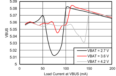
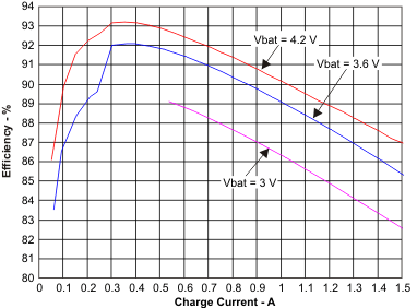
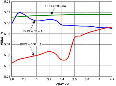
Using circuit shown in Figure 25, TA = 25°C, unless otherwise specified.
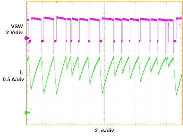
| VBUS = 5V, | VBAT = 3.5V | Charge Mode |
| Overload Operation |
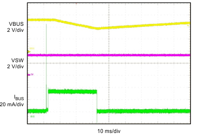
| VBUS = 5 V at 8 mA, | VBAT = 3.2V, | Iin_limit = 100 mA, |
| ICHG = 550 mA |
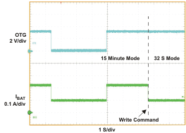
| VBUS = 5 V, VBAT = 3.1V, Iin_limit = 100/500 mA, | ||
| (OTG Control, 15 Minute Mode), Iin_limit = 100 mA | ||
| (I2C Control, 32 Second Mode) |
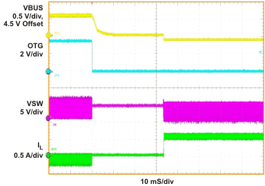
| VBUS = 4.5 V (Charge Mode) / 5.1 V | ||
| (Boost Mode), VBAT = 3.5V, IIN_LIM = 500 mA, (32S mode) |
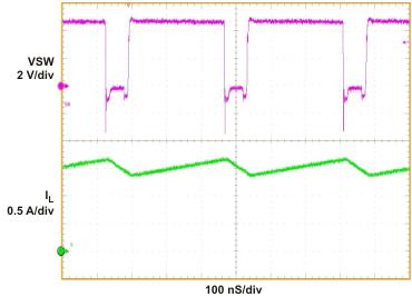
| VBUS = 5 V, | VBAT = 2.6 V, | Voreg = 4.2 V, |
| ICHG = 1550 mA |
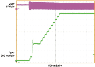
| Vin = 5 V, | VBAT = 3. 2V, | No Input Current Limit, |
| ICHG = 1550mA |
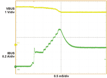
| VBUS = 5 V at 500 mA, VBAT = 3.5V, ICHG = 1550 mA, | ||
| VIN_DPM = 4.52 V | ||
| space |
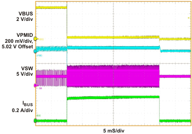
| VBUS = 5.05 V, | VBAT = 3.5V, | RLOAD (at VBUS) = 1kΩ |
| to 0.5Ω |
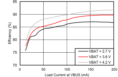
| space | ||
