SLUSB80E September 2012 – January 2018
PRODUCTION DATA.
- 1 Features
- 2 Applications
- 3 Description
- 4 Revision History
- 5 Description (Continued)
- 6 Device Comparisons
- 7 Pin Configuration and Functions
- 8 Specifications
-
9 Detailed Description
- 9.1 Overview
- 9.2 Functional Block Diagrams
- 9.3 Operational Flow Chart
- 9.4 Feature Description
- 9.5 Device Functional Modes
- 9.6 Programming
- 9.7 Register Description
- 10Application and Implementation
- 11Power Supply Recommendations
- 12Layout
- 13Device and Documentation Support
- 14Mechanical, Packaging, and Orderable Information
Package Options
Mechanical Data (Package|Pins)
- YFF|20
Thermal pad, mechanical data (Package|Pins)
Orderable Information
9 Detailed Description
9.1 Overview
For a current restricted power source, such as a USB host or hub, a high efficiency converter is critical to fully use the input power capacity for quickly charging the battery. Due to the high efficiency for a wide range of input voltages and battery voltages, the switch mode charger is a good choice for high speed charging with less power loss and better thermal management than a linear charger.
The bq24157 are highly integrated synchronous switch-mode chargers, featuring integrated FETs and small external components, targeted at extremely space-limited portable applications powered by 1-cell Li-Ion or Li-polymer battery pack. Furthermore, bq24157 also has bi-directional operation to achieve boost function for USB OTG support.
The bq24157 have three operation modes: charge mode, boost mode, and high impedance mode. In charge mode, the IC supports a precision Li-ion or Li-polymer charging system for single-cell applications. In boost mode, the IC boosts the battery voltage to VBUS for powering attached OTG devices. In high impedance mode, the IC stops charging or boosting and operates in a mode with very low current from VBUS or battery, to effectively reduce the power consumption when the portable device is in standby mode. Through I2C communication with a host, referred to as "HOST" control/mode, the IC achieves smooth transition among the different operation modes. Even when no I2C communication is available, the IC starts in default mode. During default mode operation, the charger will still charge the battery but using each register's default values.
9.2 Functional Block Diagrams
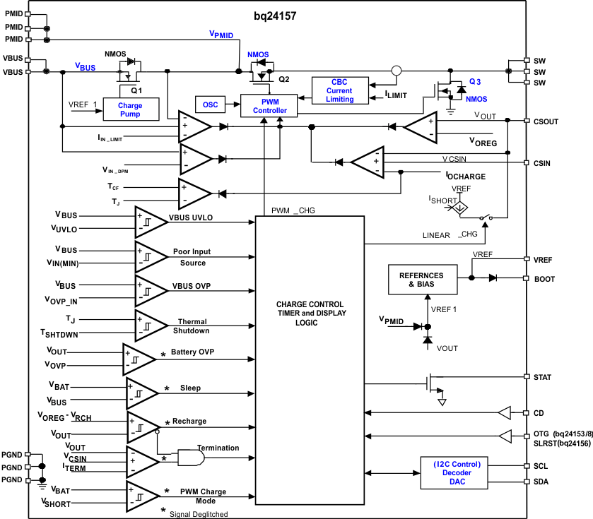 Figure 12. Function Block Diagram of bq2415x in Charge Mode
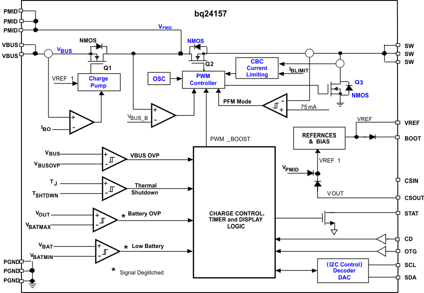 Figure 13. Function Block Diagram of bq2415x in Boost Mode
9.4 Feature Description
9.4.1 Input Voltage Protection
9.4.1.1 Input Overvoltage Protection
The IC provides a built-in input overvoltage protection to protect the device and other components against damage if the input voltage (Voltage from VBUS to PGND) goes too high. When an input overvoltage condition is detected, the IC turns off the PWM converter, sets fault status bits, and sends out a fault pulse from the STAT pin. Once VBUS drops below the input overvoltage exit threshold, the fault is cleared and charge process resumes.
9.4.1.2 Bad Adaptor Detection/Rejection
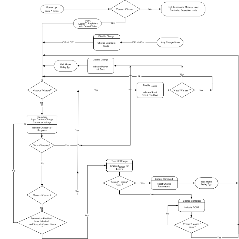
Although not shown in Figure 14, at power-on-reset (POR) of VBUS, the IC performs the bad adaptor detection by applying a current sink to VBUS. If the VBUS is higher than VIN(MIN) for 30ms, the adaptor is good and the charge process begins. Otherwise, if the VBUS drops below VIN(MIN), a bad adaptor is detected. Then, the IC disables the current sink, sends a send fault pulse in FAULT pin and sets the bad adaptor flag (B2 - B0 = 011 for Register 00H). After a delay of TINT, the IC repeats the adaptor detection process, as shown in Figure 15 and Figure 16.
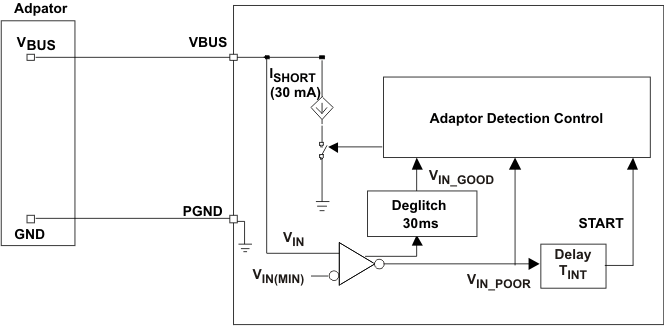 Figure 15. Bad Adaptor Detection Circuit
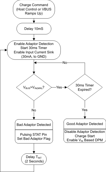 Figure 16. Bad Adaptor Detection Scheme Flow Chart
9.4.1.3 Sleep Mode
The IC enters the low-power sleep mode if the VBUS pin voltage falls below the sleep-mode entry threshold, VCSOUT+VSLP, and VBUS is higher than the bad adaptor detection threshold, VIN(MIN). This feature prevents draining the battery during the absence of VBUS. During sleep mode, both the reverse blocking switch Q1 and PWM are turned off.
9.4.1.4 Input Voltage Based DPM (Special Charger Voltage Threshold)
During the charging process, if the input power source is not able to support the programmed or default charging current, the VBUS voltage will decrease. Once the VBUS drops to VIN_DPM (default 4.52V), the charge current begins to taper down to prevent any further drop of VBUS. When the IC enters this mode, the charge current is lower than the set value and the special charger bit is set (B4 in Register 05H). This feature makes the IC compatible with adapters having different current capabilities.
9.4.2 Battery Protection
9.4.2.1 Output Overvoltage Protection
The IC provides a built-in overvoltage protection to protect the device and other components against damage if the battery voltage goes too high, as when the battery is suddenly removed. When an overvoltage condition is detected, the IC turns off the PWM converter, sets fault status bits, and sends out a fault pulse from the STAT pin. Once V(CSOUT) drops to the battery overvoltage exit threshold, the fault is cleared and charge process resumes.
9.4.2.2 Battery Detection at Power Up in DEFAULT Mode
bq24157 also has a unique battery detection scheme during the start up of the charger. At VBUS power up, bq24157 starts a 262-ms timer when exiting from short circuit mode to PWM charge mode. If the battery voltage is charged above the recharge threshold (VOREG-VRCH) when the 262-ms timer expired, bq2157 will not consider the battery present; then stop charging, and go to high impedance mode immediately. However, if the battery voltage is still below the recharge threshold when the 262-ms timer expires, the charging process will continue as normal battery charging process.
9.4.2.3 Battery Short Protection
During the normal charging process, if the battery voltage is lower than the short-circuit threshold, VSHORT, the charger operates in short circuit mode with a lower charge rate of ISHORT.
9.4.2.4 Battery Detection in Host Mode
For applications with removable battery packs, the IC provides a battery absent detection scheme to reliably detect insertion or removal of battery packs.
During the normal charging process with host control, once the voltage at the CSOUT pin is above the battery recharge threshold, VOREG - VRCH, and the termination charge current is detected, the IC turns off the PWM charge and enables a discharge current, IDETECT, for a period of tDETECT, (262 ms typical) then checks the battery voltage. If the battery voltage is still above the recharge threshold after tDETECT, the battery is present. On the other hand, if the battery voltage is below the battery recharge threshold, the battery is absent. Under this condition, the charge parameters (such as input current limit) are reset to the default values and charge resumes after a delay of TINT. This function ensures that the charge parameters are reset whenever the battery is replaced.
9.4.4 USB Friendly Power Up
The default control bits set the charging current and regulation voltage low as a safety feature to avoid violating USB spec and over-charging any of the Li-Ion chemistries, while the host has lost communication. The input current limiting is described below.
9.4.5 Input Current Limiting At Power Up
The input current sensing circuit and control loop are integrated into the IC. When operating in default mode, the OTG pin logic level sets the input current limit to 100mA for a logic low and 500mA for a logic high. In host mode, the input current limit is set by the programmed control bits in register 01H.
9.5 Device Functional Modes
9.5.1 Charge Mode Operation
9.5.1.1 Charge Profile
Once a good battery with voltage below the recharge threshold has been inserted and a good adapter is attached, the bq24157 enters charge mode. In charge mode, the IC has five control loops to regulate input voltage, input current, charge current, charge voltage and device junction temperature. During the charging process, all five loops are enabled and the one that is dominant takes control. The IC supports a precision Li-ion or Li-polymer charging system for single-cell applications. Figure 17 (a) indicates a typical charge profile without input current regulation loop. It is the traditional CC/CV charge curve, while Figure 17(b) shows a typical charge profile when input current limiting loop is dominant during the constant current mode. In this case, the charge current is higher than the input current so the charge process is faster than the linear chargers. The input voltage threshold for DPM loop, input current limits, charge current, termination current, and charge voltage are all programmable using I2C interface.
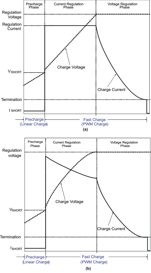 Figure 17. Typical Charging Profile for (a) without Input Current Limit, and (b) with Input Current Limit
9.5.2 PWM Controller in Charge Mode
The IC provides an integrated, fixed 3 MHz frequency voltage-mode controller to regulate charge current or voltage. This type of controller is used to improve line transient response, thereby, simplifying the compensation network used for both continuous and discontinuous current conduction operation. The voltage and current loops are internally compensated using a Type-III compensation scheme that provides enough phase margin for stable operation, allowing the use of small ceramic capacitors with a low ESR. The device operates between 0% to 99.5% duty cycles.
The IC has back to back common-drain N-channel FETs at the high side and one N-channel FET at low side. The input N-FET (Q1) prevents battery discharge when VBUS is lower than VCSOUT. The second high-side N-FET (Q2) is the switching control switch. A charge pump circuit is used to provide gate drive for Q1, while a bootstrap circuit with an external bootstrap capacitor is used to supply the gate drive voltage for Q2.
Cycle-by-cycle current limit is sensed through the FETs Q2 and Q3. The threshold for Q2 is set to a nominal 2.4-A peak current. The low-side FET (Q3) also has a current limit that decides if the PWM Controller will operate in synchronous or non-synchronous mode. This threshold is set to 100mA and it turns off the low-side N-channel FET (Q3) before the current reverses, preventing the battery from discharging. Synchronous operation is used when the current of the low-side FET is greater than 100mA to minimize power losses.
9.5.3 Battery Charging Process
At the beginning of precharge, while battery voltage is below the V(SHORT) threshold, the IC applies a short-circuit current, I(SHORT), to the battery. When the battery voltage is above VSHORT and below VOREG, the charge current ramps up to fast charge current, IOCHARGE, or a charge current that corresponds to the input current of IIN_LIMIT. The slew rate for fast charge current is controlled to minimize the current and voltage over-shoot during transient. Both the input current limit, IIN_LIMIT, and fast charge current, IOCHARGE, can be set by the host. Once the battery voltage reaches the regulation voltage, VOREG, the charge current is tapered down as shown in Figure 17. The voltage regulation feedback occurs by monitoring the battery-pack voltage between the CSOUT and PGND pins. In HOST mode, the regulation voltage is adjustable (3.5V to 4.44V) and is programmed through I2C interface. In 15-minute mode, the regulation voltage is fixed at 3.54V.
The IC monitors the charging current during the voltage regulation phase. If termination is enabled, during the normal charging process with HOST control, once the voltage at the CSOUT pin is above the battery recharge threshold, VOREG - VRCH for the 32-ms (typical) deglitch period, and the termination charge current ITERM is detected, the IC turns off the PWM charge and enables a discharge current, IDETECT, for a period of tDETECT (262-ms typical), then checks the battery voltage. If the battery voltage is still above the recharge threshold after tDETECT, the battery charging is complete. The battery detection routine is used to ensure termination did not occur because the battery was removed. After 40ms (typical) for synchronization purposes of the EOC state and the counter, the status bit and pin are updated to indicate charging has completed. The termination current level is programmable. To disable the charge current termination, the host can set the charge termination bit (I_Term) of charge control register to 0, refer to I2C section for detail.
A new charge cycle is initiated when one of the following conditions is detected:
- The battery voltage falls below the V(OREG) – V(RCH) threshold.
- VBUS Power-on reset (POR), if battery voltage is below the V(LOWV) threshold.
- CE bit toggle or RESET bit is set (Host controlled)
9.5.4 Thermal Regulation and Protection
To prevent overheating of the chip during the charging process, the IC monitors the junction temperature, TJ, of the die and begins to taper down the charge current once TJ reaches the thermal regulation threshold, TCF. The charge current is reduced to zero when the junction temperature increases approximately 10°C above TCF. In any state, if TJ exceeds TSHTDWN, the IC suspends charging. In thermal shutdown mode, PWM is turned off and all timers are frozen. Charging resumes when TJ falls below TSHTDWN by approximately 10°C.
9.5.5 Charge Status Output, STAT Pin
The STAT pin is used to indicate operation conditions. STAT is pulled low during charging when EN_STAT bit in control register (00H) is set to “1”. Under other conditions, STAT pin behaves as a high impedance (open-drain) output. Under fault conditions, a 128-µs pulse will be sent out to notify the host. The status of STAT pin at different operation conditions is summarized in Table 1. The STAT pin can be used to drive an LED or communicate to the host processor.
Table 1. STAT Pin Summary
| CHARGE STATE | STAT |
|---|---|
| Charge in progress and EN_STAT=1 | Low |
| Other normal conditions | Open-drain |
| Charge mode faults: Timer fault, sleep mode, VBUS or battery overvoltage, poor input source, VBUS UVLO, no battery, thermal shutdown | 128-μs pulse, then open-drain |
| Boost mode faults: Timer fault, over load, VBUS or battery overvoltage, low battery voltage, thermal shutdown | 128-μs pulse, then open-drain |
9.5.6 Control Bits in Charge Mode
9.5.6.1 CE Bit (Charge Mode)
The CE bit in the control register is used to disable or enable the charge process. A low logic level (0) on this bit enables the charge and a high logic level (1) disables the charge.
9.5.6.2 RESET Bit
The RESET bit in the control register is used to reset all the charge parameters. Writing ‘1” to the RESET bit will reset all the charge parameters to default values except the safety limit register, and RESET bit is automatically cleared to zero once the charge parameters get reset. It is designed for charge parameter reset before charge starts and it is not recommended to set the RESET bit while charging or boosting are in progress.
9.5.6.3 OPA_Mode Bit
OPA_MODE is the operation mode control bit. When OPA_MODE = 0, the IC operates as a charger if HZ_MODE is set to "0", refer to Table 2 for detail. When OPA_MODE=1 and HZ_MODE=0, the IC operates in boost mode.
Table 2. Operation Mode Summary
| OPA_MODE | HZ_MODE | OPERATION MODE |
|---|---|---|
| 0 | 0 | Charge (no fault) Charge configure (fault, Vbus > UVLO) High impedance (Vbus < UVLO) |
| 1 | 0 | Boost (no faults) Any fault go to charge configure mode |
| X | 1 | High impedance |
9.5.7 Control Pins in Charge Mode
9.5.7.1 CD Pin (Charge Disable)
The CD pin is used to disable the charging process. When the CD pin is low, charge is enabled. When the CD pin is high, charge is disabled and the charger enters high impedance (Hi-Z) mode.
9.5.8 BOOST Mode Operation
In host mode, when OTG pin is high (and OTG_EN bit is high thereby enabling OTG functionality) or the operation mode bit (OPA_MODE) is set to 1, the device operates in boost mode and delivers the power to VBUS from the battery. In normal boost mode converts the battery voltage to VBUS-B (about 5.05V) and delivers a current as much as IBO (about 200mA) to support other USB OTG devices connected to the USB connector.
9.5.8.1 PWM Controller in Boost Mode
Similar to charge mode operation, in boost mode, the IC provides an integrated, fixed 3 MHz frequency voltage-mode controller to regulate output voltage at PMID pin (VPMID). The voltage control loop is internally compensated using a Type-III compensation scheme that provides enough phase margin for stable operation with a wide load range and battery voltage range.
In boost mode, the input N-FET (Q1) prevents battery discharge when VBUS pin is over loaded. Cycle-by-cycle current limit is sensed through the internal sense FET for Q3. The cycle-by-cycle current limit threshold for Q3 is set to a nominal 1.0-A peak current. Synchronous operation is used in PWM mode to minimize power losses.
9.5.8.2 Boost Start Up
To prevent the inductor saturation and limit the inrush current, a soft-start control is applied during the boost start up.
9.5.8.3 PFM Mode at Light Load
In boost mode, under light load conditions, the IC operates in pulse skipping mode (PFM mode) to reduce the power loss and improve the converter efficiency. During boosting, the PWM converter is turned off once the inductor current is less than 75mA; and the PWM is turned back on only when the voltage at PMID pin drops to about 99.5% of the rated output voltage. A unique pre-set circuit is used to make the smooth transition between PWM and PFM mode.
9.5.8.4 Protection in Boost Mode
9.5.8.4.1 Output Overvoltage Protection
The IC provides a built-in over-voltage protection to protect the device and other components against damage if the VBUS voltage goes too high. When an over-voltage condition is detected, the IC turns off the PWM converter, resets OPA_MODE bit to 0, sets fault status bits, and sends out a fault pulse from the STAT pin. Once VBUS drops to the normal level, the boost starts after host sets OPA_MODE to “1” or OTG pin stays in active status.
9.5.8.4.2 Output Overload Protection
The IC provides a built-in over-load protection to prevent the device and battery from damage when VBUS is over loaded. Once the over load condition is detected, Q1 operates in linear mode to limit the output current. If the over load condition lasts for more than 30ms, the over-load fault is detected. When an over-load condition is detected, the IC turns off the PWM converter, resets OPA_MODE bit to 0, sets fault status bits and sends out fault pulse in STAT pin. The boost will not start until the host clears the fault register.
9.5.8.4.3 Battery Overvoltage Protection
During boosting, when the battery voltage is above the battery over voltage threshold, VBATMAX, or below the minimum battery voltage threshold, VBATMIN, the IC turns off the PWM converter, resets OPA_MODE bit to 0, sets fault status bits and sends out fault pulse in STAT pin. Once the battery voltage goes above VBATMIN, the boost will start after the host sets OPA_MODE to “1” or OTG pin stays in active status.
9.5.8.5 STAT Pin in Boost Mode
During normal boosting operation, the STAT pin behaves as a high impedance (open-drain) output. Under fault conditions, a 128-μs pulse is sent out to notify the host.
9.5.9 High Impedance (Hi-Z) Mode
In Hi-Z mode, the charger stops charging and enters a low quiescent current state to conserve power. Taking the CD pin high causes the charger to enter Hi-Z mode. When in default mode and the CD pin is low, the charger automatically enters Hi-Z mode if
- VBUS > UVLO and a battery with VBAT > VLOWV is inserted, or
- VBUS falls below UVLO.
When in HOST mode and the CD is low, the charger can be placed into Hi-Z mode if the HZ-MODE control bit is set to “1” and OTG pin is not in active status.
In order to exit Hi-Z mode, the CD pin must be low, VBUS must be higher than UVLO and the HOST must write a "0" to the HZ-MODE control bit.
9.6 Programming
9.6.1 Serial Interface Description
I2C is a 2-wire serial interface developed by Philips Semiconductor (see I2C-Bus Specification, Version 2.1, January 2000). The bus consists of a data line (SDA) and a clock line (SCL) with pull-up structures. When the bus is idle, both SDA and SCL lines are pulled high. All the I2C compatible devices connect to the I2C bus through open drain I/O pins, SDA and SCL. A master device, usually a microcontroller or a digital signal processor, controls the bus. The master is responsible for generating the SCL signal and device addresses. The master also generates specific conditions that indicate the START and STOP of data transfer. A slave device receives and/or transmits data on the bus under control of the master device.
The IC works as a slave and is compatible with the following data transfer modes, as defined in the I2C-Bus Specification: standard mode (100 kbps), fast mode (400 kbps), and high-speed mode (up to 3.4 Mbps in write mode). The interface adds flexibility to the battery charge solution, enabling most functions to be programmed to new values depending on the instantaneous application requirements. Register contents remain intact as long as supply voltage remains above 2.2 V (typical). I2C is asynchronous, which means that it runs off of SCL. The device has no noise or glitch filtering on SCL, so SCL input needs to be clean. Therefore, it is recommended that SDA changes while SCL is LOW.
The data transfer protocol for standard and fast modes is the same; therefore, they are referred to as F/S-mode in this document. The protocol for high-speed mode is different from the F/S-mode, and it is referred to as HS-mode. The bq24157B device supports 7-bit addressing only. The device 7-bit address is defined as ‘1101010’ (6AH).
9.6.1.1 F/S Mode Protocol
The master initiates data transfer by generating a start condition. The start condition is when a high-to-low transition occurs on the SDA line while SCL is high, as shown in Figure 18. All I2C-compatible devices should recognize a start condition.
 Figure 18. START and STOP Condition
The master then generates the SCL pulses, and transmits the 8-bit address and the read/write direction bit R/W on the SDA line. During all transmissions, the master ensures that data is valid. A valid data condition requires the SDA line to be stable during the entire high period of the clock pulse (see Figure 19). All devices recognize the address sent by the master and compare it to their internal fixed addresses. Only the slave device with a matching address generates an acknowledge (see Figure 19) by pulling the SDA line low during the entire high period of the ninth SCL cycle. Upon detecting this acknowledge, the master knows that communication link with a slave has been established.
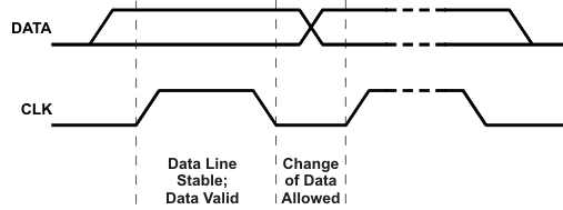 Figure 19. Bit Transfer on the Serial Interface
The master generates further SCL cycles to either transmit data to the slave (R/W bit 1) or receive data from the slave (R/W bit 0). In either case, the receiver needs to acknowledge the data sent by the transmitter. So an acknowledge signal can either be generated by the master or by the slave, depending on which one is the receiver. The 9-bit valid data sequences consisting of 8-bit data and 1-bit acknowledge can continue as long as necessary. To signal the end of the data transfer, the master generates a stop condition by pulling the SDA line from low to high while the SCL line is high (see Figure 21). This releases the bus and stops the communication link with the addressed slave. All I2C compatible devices must recognize the stop condition. Upon the receipt of a stop condition, all devices know that the bus is released, and they wait for a start condition followed by a matching address. If a transaction is terminated prematurely, the master needs to send a STOP condition to prevent the slave I2C logic from getting stuck in a bad state. Attempting to read data from register addresses not listed in this section will result in FFh being read out.
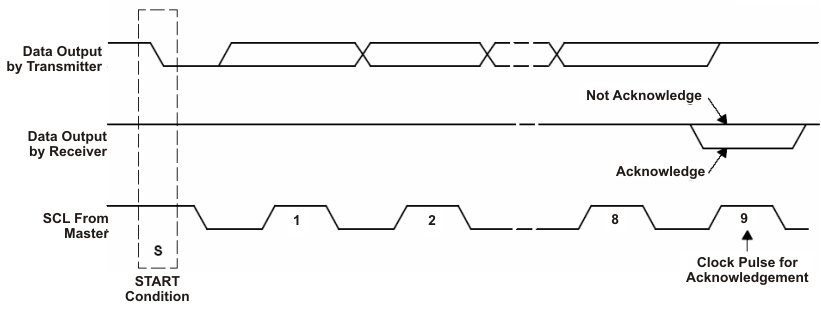 Figure 20. Acknowledge on the I2C Bus™
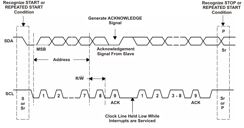 Figure 21. Bus Protocol
9.6.1.2 H/S Mode Protocol
When the bus is idle, both SDA and SCL lines are pulled high by the pull-up devices.
The master generates a start condition followed by a valid serial byte containing HS master code 00001XXX. This transmission is made in F/S-mode at no more than 400 Kbps. No device is allowed to acknowledge the HS master code, but all devices must recognize it and switch their internal setting to support 3.4-Mbps operation.
The master then generates a repeated start condition (a repeated start condition has the same timing as the start condition). After this repeated start condition, the protocol is the same as F/S-mode, except that transmission speeds up to 3.4 Mbps are allowed. A stop condition ends the HS-mode and switches all the internal settings of the slave devices to support the F/S-mode. Instead of using a stop condition, repeated start conditions should be used to secure the bus in HS-mode. If a transaction is terminated prematurely, the master needs sending a STOP condition to prevent the slave I2C logic from getting stuck in a bad state.
Attempting to read data from register addresses not listed in this section results in FFh being read out.
9.6.1.3 I2C Update Sequence
The IC requires a start condition, a valid I2C address, a register address byte, and a data byte for a single update. After the receipt of each byte, the IC acknowledges by pulling the SDA line low during the high period of a single clock pulse. A valid I2C address selects the IC. The IC performs an update on the falling edge of the acknowledge signal that follows the LSB byte.
For the first update, the IC requires a start condition, a valid I2C address, a register address byte, a data byte. For all consecutive updates, The IC needs a register address byte, and a data byte. Once a stop condition is received, the IC releases the I2C bus, and awaits a new start conditions.
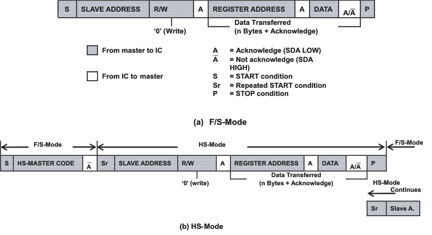 Figure 22. Data Transfer Format in F/S Mode and H/S Mode
9.6.1.4 Slave Address Byte
| MSB | LSB |
| X | 1 | 1 | 0 | 1 | 0 | 1 | 1 |
The slave address byte is the first byte received following the START condition from the master device.
9.6.1.5 Register Address Byte
| MSB | LSB |
| 0 | 0 | 0 | 0 | 0 | D2 | D1 | D0 |
Following the successful acknowledgment of the slave address, the bus master will send a byte to the IC, which contains the address of the register to be accessed. The IC contains five 8-bit registers accessible via a bidirectional I2C-bus interface. Among them, four internal registers have read and write access; and one has only read access.
9.7 Register Description
Table 3. Status/Control Register (Read/Write)
Memory Location: 00, Reset State: x1xx 0xxx
| BIT | NAME | READ/WRITE | FUNCTION |
|---|---|---|---|
| B7 (MSB) | TMR_RST/OTG | Read/Write | Write: TMR_RST function, write "1" to reset the safety timer (auto clear) Read: OTG pin status, 0-OTG pin at Low level, 1-OTG pin at High level |
| B6 | EN_STAT | Read/Write | 0-Disable STAT pin function, 1-Enable STAT pin function (default 1) |
| B5 | STAT2 | Read Only | 00-Ready, 01-Charge in progress, 10-Charge done, 11-Fault |
| B4 | STAT1 | Read Only | |
| B3 | BOOST | Read Only | 1-Boost mode, 0-Not in boost mode |
| B2 | FAULT_3 | Read Only | Charge mode: 000-Normal, 001-VBUS OVP, 010-Sleep mode, 011-Bad Adaptor or VBUS<VUVLO, 100-Output OVP, 101-Thermal shutdown, 110-Timer fault, 111-No battery Boost mode: 000-Normal, 001-VBUS OVP, 010-Over load, 011-Battery voltage is too low, 100-Battery OVP, 101-Thermal shutdown, 110-Timer fault, 111-NA |
| B1 | FAULT_2 | Read Only | |
| B0 (LSB) | FAULT_1 | Read Only |
Table 4. Control Register (Read/Write)
Memory Location: 01, Reset State: 0011 0000
| BIT | NAME | READ/WRITE | FUNCTION |
|---|---|---|---|
| B7 (MSB) | Iin_Limit_2 | Read/Write | 00-USB host with 100-mA current limit, 01-USB host with 500-mA current limit, 10-USB host/charger with 800-mA current limit, 11-No input current limit |
| B6 | Iin_Limit_1 | Read/Write | |
| B5 | V(LOWV_2) (1) | Read/Write | Weak battery voltage threshold: 200mV step (default 1) |
| B4 | V(LOWV_1) (1) | Read/Write | Weak battery voltage threshold: 100mV step (default 1) |
| B3 | TE | Read/Write | 1-Enable charge current termination, 0-Disable charge current termination (default 0) |
| B2 | CE | Read/Write | 1-Charger is disabled, 0-Charger enabled (default 0) |
| B1 | HZ_MODE | Read/Write | 1-High impedance mode, 0-Not high impedance mode (default 0) |
| B0 (LSB) | OPA_MODE | Read/Write | 1-Boost mode, 0-Charger mode (default 0) |
Table 5. Control/Battery Voltage Register (Read/Write)
Memory Location: 02, Reset State: 0000 1010
| BIT | NAME | READ/WRITE | FUNCTION |
|---|---|---|---|
| B7 (MSB) | VO(REG5) | Read/Write | Battery Regulation Voltage: 640 mV step (default 0) |
| B6 | VO(REG4) | Read/Write | Battery Regulation Voltage: 320 mV step (default 0) |
| B5 | VO(REG3) | Read/Write | Battery Regulation Voltage: 160 mV step (default 0) |
| B4 | VO(REG2) | Read/Write | Battery Regulation Voltage: 80 mV step (default 0) |
| B3 | VO(REG1) | Read/Write | Battery Regulation Voltage: 40 mV step (default 1) |
| B2 | VO(REG0) | Read/Write | Battery Regulation Voltage: 20 mV step (default 0) |
| B1 | OTG_PL | Read/Write | 1-OTG Boost Enable with High level, 0-OTG Boost Enable with Low level (default 1); not applicable to OTG pin control of current limit at POR in default mode |
| B0 (LSB) | OTG_EN | Read/Write | 1-Enable OTG Pin in HOST mode, 0-Disable OTG pin in HOST mode (default 0), not applicable to OTG pin control of current limit at POR in default mode |
- Charge voltage range is 3.5 V to 4.44 V with the offset of 3.5 V and steps of 20 mV (default 3.54 V), using bits B2-B7.
Table 6. Vender/Part/Revision Register (Read only)
Memory Location: 03, Reset State: 0101 000x
| BIT | NAME | READ/WRITE | FUNCTION |
|---|---|---|---|
| B7 (MSB) | Vender2 | Read Only | Vender Code: bit 2 (default 0) |
| B6 | Vender1 | Read Only | Vender Code: bit 1 (default 1) |
| B5 | Vender0 | Read Only | Vender Code: bit 0 (default 0) |
| B4 | PN1 | Read Only | For I2C Address 6AH: 01–NA, 10–bq24157, 11–NA. |
| B3 | PN0 | Read Only | |
| B2 | Revision2 | Read Only | 011: Revision 1.0; 001: Revision 1.1; 100-111: Future Revisions |
| B1 | Revision1 | Read Only | |
| B0 (LSB) | Revision0 | Read Only |
Table 7. Battery Termination/Fast Charge Current Register (Read/Write)
Memory Location: 04, Reset State: 0000 0001
| BIT | NAME | READ/WRITE | FUNCTION |
|---|---|---|---|
| B7 (MSB) | Reset | Read/Write | Write: 1-Charger in reset mode, 0-No effect, Read: always get "0" |
| B6 | VI(CHRG3) (1) | Read/Write | Charge current sense voltage: 27.2 mV step |
| B5 | VI(CHRG2) (1) | Read/Write | Charge current sense voltage: 13.6 mV step |
| B4 | VI(CHRG1) (1) | Read/Write | Charge current sense voltage: 6.8 mV step |
| B3 | VI(CHRG0) (1) | Read/Write | NA |
| B2 | VI(TERM2) (2) | Read/Write | Termination current sense voltage: 13.6 mV step (default 0) |
| B1 | VI(TERM1) (2) | Read/Write | Termination current sense voltage: 6.8 mV step (default 0) |
| B0 (LSB) | VI(TERM0) (2) | Read/Write | Termination current sense voltage: 3.4 mV step (default 1) |
- Charge current sense voltage offset is 37.4 mV and default charge current is 550 mA, if 68-mΩ sensing resistor is used and LOW_CHG=0.
Table 8. Special Charger Voltage/Enable Pin Status Register
Memory location: 05, Reset state: 000X X100
- Special charger voltage offset is 4.2 V and default special charger voltage is 4.52 V.
Table 9. Safety Limit Register (READ/WRITE, Write only once after reset!)
Memory location: 06, Reset state: 01000000
| BIT | NAME | READ/WRITE | FUNCTION |
|---|---|---|---|
| B7 (MSB) | VMCHRG3 (1) | Read/Write | Maximum charge current sense voltage: 54.4 mV step (default 0) (2) |
| B6 | VMCHRG2 (1) | Read/Write | Maximum charge current sense voltage: 27.2 mV step (default 1) |
| B5 | VMCHRG1 (1) | Read/Write | Maximum charge current sense voltage: 13.6 mV step (default 0) |
| B4 | VMCHRG0 (1) | Read/Write | Maximum charge current sense voltage: 6.8 mV step (default 0) |
| B3 | VMREG3 | Read/Write | Maximum battery regulation voltage: 160 mV step (default 0) |
| B2 | VMREG2 | Read/Write | Maximum battery regulation voltage: 80 mV step (default 0) |
| B1 | VMREG1 | Read/Write | Maximum battery regulation voltage: 40 mV step (default 0) |
| B0 (LSB) | VMREG0 | Read/Write | Maximum battery regulation voltage: 20 mV step (default 0) |
- Maximum charge current sense voltage offset is 37.4 mV (550 mA), default at 64.6 mV (950 mA) and the maximum charge current option is 1.55 A (105.4 mV), if 55-mΩ sensing resistor is used.
- Maximum battery regulation voltage offset is 4.2V (default at 4.2 V) and maximum battery regulation voltage option is 4.44V.
- Memory location 06H resets only when V(CSOUT) drops below either 1) V(SHORT) threshold (typ. 2.05 V) if VBUS > V(UVLO) or 2) the digital reset threshold of 2.4 V typical if VBUS < V(UVLO). Programmed values in the safety limit register exclude higher values from memory locations 02 (battery regulation voltage), and from memory location 04 (fast charge current) from being successfully written.
- If host accesses (write command) to some other register before Safety limit register, the safety default values are used.
