SLUSB80E September   2012  – January 2018

PRODUCTION DATA.  

  1. Features
  2. Applications
  3. Description
  4. Revision History
  5. Description (Continued)
  6. Device Comparisons
  7. Pin Configuration and Functions
  8. Specifications
    1. 8.1 Absolute Maximum Ratings
    2. 8.2 ESD Ratings
    3. 8.3 Recommended Operating Conditions
    4. 8.4 Thermal Information
    5. 8.5 Electrical Characteristics
    6. 8.6 Timing Requirements
    7. 8.7 Typical Characteristics
  9. Detailed Description
    1. 9.1 Overview
    2. 9.2 Functional Block Diagrams
    3. 9.3 Operational Flow Chart
    4. 9.4 Feature Description
      1. 9.4.1 Input Voltage Protection
        1. 9.4.1.1 Input Overvoltage Protection
        2. 9.4.1.2 Bad Adaptor Detection/Rejection
        3. 9.4.1.3 Sleep Mode
        4. 9.4.1.4 Input Voltage Based DPM (Special Charger Voltage Threshold)
      2. 9.4.2 Battery Protection
        1. 9.4.2.1 Output Overvoltage Protection
        2. 9.4.2.2 Battery Detection at Power Up in DEFAULT Mode
        3. 9.4.2.3 Battery Short Protection
        4. 9.4.2.4 Battery Detection in Host Mode
      3. 9.4.3 DEFAULT Mode
      4. 9.4.4 USB Friendly Power Up
      5. 9.4.5 Input Current Limiting At Power Up
    5. 9.5 Device Functional Modes
      1. 9.5.1 Charge Mode Operation
        1. 9.5.1.1 Charge Profile
      2. 9.5.2 PWM Controller in Charge Mode
      3. 9.5.3 Battery Charging Process
      4. 9.5.4 Thermal Regulation and Protection
      5. 9.5.5 Charge Status Output, STAT Pin
      6. 9.5.6 Control Bits in Charge Mode
        1. 9.5.6.1 CE Bit (Charge Mode)
        2. 9.5.6.2 RESET Bit
        3. 9.5.6.3 OPA_Mode Bit
      7. 9.5.7 Control Pins in Charge Mode
        1. 9.5.7.1 CD Pin (Charge Disable)
      8. 9.5.8 BOOST Mode Operation
        1. 9.5.8.1 PWM Controller in Boost Mode
        2. 9.5.8.2 Boost Start Up
        3. 9.5.8.3 PFM Mode at Light Load
        4. 9.5.8.4 Protection in Boost Mode
          1. 9.5.8.4.1 Output Overvoltage Protection
          2. 9.5.8.4.2 Output Overload Protection
          3. 9.5.8.4.3 Battery Overvoltage Protection
        5. 9.5.8.5 STAT Pin in Boost Mode
      9. 9.5.9 High Impedance (Hi-Z) Mode
    6. 9.6 Programming
      1. 9.6.1 Serial Interface Description
        1. 9.6.1.1 F/S Mode Protocol
        2. 9.6.1.2 H/S Mode Protocol
        3. 9.6.1.3 I2C Update Sequence
        4. 9.6.1.4 Slave Address Byte
        5. 9.6.1.5 Register Address Byte
    7. 9.7 Register Description
  10. 10Application and Implementation
    1. 10.1 Application Information
      1. 10.1.1 Typical Application
        1. 10.1.1.1 Design Requirements
        2. 10.1.1.2 Detailed Design Procedure
      2. 10.1.2 Charge Current Sensing Resistor Selection Guidelines
      3. 10.1.3 Output Inductor and Capacitance Selection Guidelines
    2. 10.2 Typical Performance Curves
  11. 11Power Supply Recommendations
    1. 11.1 System Load After Sensing Resistor
      1. 11.1.1 The Advantages:
      2. 11.1.2 Design Requirements and Potential Issues:
  12. 12Layout
    1. 12.1 Layout Guidelines
    2. 12.2 Layout Example
  13. 13Device and Documentation Support
    1. 13.1 Documentation Support
      1. 13.1.1 Third-Party Products Disclaimer
    2. 13.2 Receiving Notification of Documentation Updates
    3. 13.3 Community Resources
    4. 13.4 Trademarks
    5. 13.5 Electrostatic Discharge Caution
    6. 13.6 Glossary
  14. 14Mechanical, Packaging, and Orderable Information
    1. 14.1 Package Summary
      1. 14.1.1 Chip Scale Packaging Dimensions

Package Options

Mechanical Data (Package|Pins)
Thermal pad, mechanical data (Package|Pins)
Orderable Information

Mechanical, Packaging, and Orderable Information

The following pages include mechanical, packaging, and orderable information. This information is the most current data available for the designated devices. This data is subject to change without notice and revision of this document. For browser-based versions of this data sheet, refer to the left-hand navigation.

Package Summary

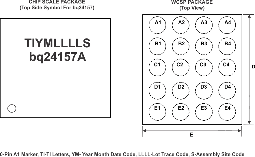
bq24157 package_sum2_lusb80.gif

Chip Scale Packaging Dimensions

The bq24157 device is available in a 20-bump chip scale package (YFF, NanoFree™).

The package dimensions are:

D E
Max = 2.17mm Max = 2.03 mm
Min = 2.11 mm Min = 1.97 mm