SLUSAW5B January 2012 – December 2014
PRODUCTION DATA.
- 1 Features
- 2 Applications
- 3 Description
- 4 Revision History
- 5 Description (Continued)
- 6 Device Comparison Table
- 7 Pin Configuration and Functions
- 8 Specifications
-
9 Detailed Description
- 9.1 Overview
- 9.2 Functional Block Diagram
- 9.3
Feature Description
- 9.3.1
Device Power Up
- 9.3.1.1 Power-On-Reset (POR)
- 9.3.1.2 Power Up from Battery without DC Source
- 9.3.1.3
Power Up from DC Source
- 9.3.1.3.1 REGN LDO
- 9.3.1.3.2 Input Source Qualification
- 9.3.1.3.3 Input Current Limit Detection
- 9.3.1.3.4 D+/D- Detection Sets Input Current Limit in bq24190
- 9.3.1.3.5 PSEL/OTG Pins Set Input Current Limit in bq24192, bq24192I
- 9.3.1.3.6 HIZ State wth 100mA USB Host
- 9.3.1.3.7 Force Input Current Limit Detection
- 9.3.1.4 Converter Power-Up
- 9.3.1.5 Boost Mode Operation from Battery
- 9.3.2 Power Path Management
- 9.3.3 Battery Charging Management
- 9.3.4 Status Outputs (PG, STAT, and INT)
- 9.3.5 Protections
- 9.3.6 Serial Interface
- 9.3.1
Device Power Up
- 9.4 Device Functional Modes
- 9.5
Register Map
- 9.5.1
I2C Registers
- 9.5.1.1 Input Source Control Register REG00 (bq24190, bq24192 reset = 00110000, or 30; bq24192I reset = 00111000, or 38)
- 9.5.1.2 Power-On Configuration Register REG01 (reset = 00011011, or 1B)
- 9.5.1.3 Charge Current Control Register REG02 (bq24190, bq24192 reset = 01100000, or 60; bq24192I reset = 00100000, or 20)
- 9.5.1.4 Pre-Charge/Termination Current Control Register REG03 (reset = 00010001, or 11)
- 9.5.1.5 Charge Voltage Control Register REG04 (bq24190, bq241192 reset = 10110010, or B2; bq24192I reset = 10011010, or 9A)
- 9.5.1.6 Charge Termination/Timer Control Register REG05 (reset = 10011010, or 9A)
- 9.5.1.7 IR Compensation / Thermal Regulation Control Register REG06 (reset = 00000011, or 03)
- 9.5.1.8 Misc Operation Control Register REG07 (reset = 01001011, or 4B)
- 9.5.1.9 System Status Register REG08
- 9.5.1.10 Fault Register REG09
- 9.5.1.11 Vender / Part / Revision Status Register REG0A (bq24190 reset = 00100011, or 23; bq24192 reset = 00101011, or 2B; bq24192I reset = 00001011, or 0B)
- 9.5.1
I2C Registers
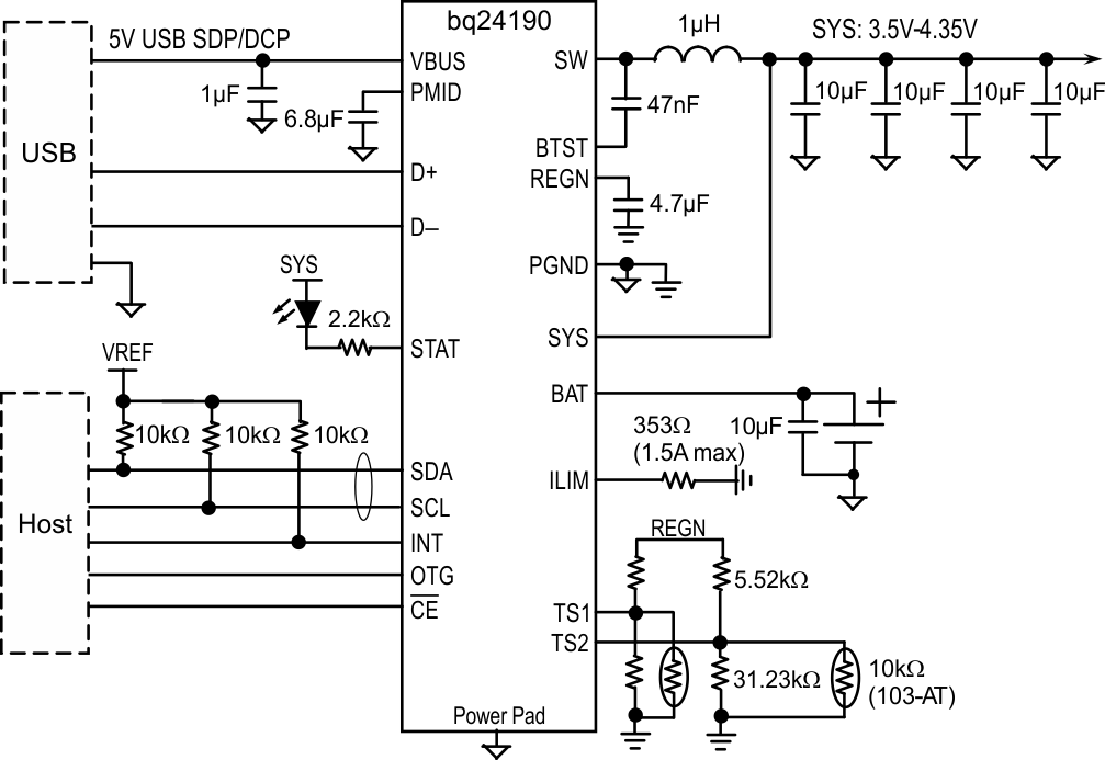
- 10Application and Implementation
- 11Power Supply Recommendations
- 12Layout
- 13Device and Documentation Support
- 14Mechanical, Packaging, and Orderable Information
Package Options
Mechanical Data (Package|Pins)
- RGE|24
Thermal pad, mechanical data (Package|Pins)
- RGE|24
Orderable Information
1 Features
- High Efficiency 4.5-A Switch Mode Charger
- 92% Charge Efficiency at 2 A, 90% at 4 A
- Accelerate Charge Time by Battery Path Impedance Compensation
- Compatible with MaxLife Technology for Faster Charging When Used in Conjunction With bq27531
- Highest Battery Discharge Efficiency with 12-mΩ Battery Discharge MOSFET up to 9-A Discharge Current
- Single Input USB-compliant/Adapter Charger
- USB Host or Charging Port D+/D- Detection Compatible to USB Battery Charger Spec 1.2
- Input Voltage and Current Limit Supports USB2.0 and USB3.0
- Input Current Limit: 100 mA, 150 mA, 500 mA, 900 mA, 1.2 A, 1.5 A, 2 A and 3 A
- 3.9-V to 17-V Input Operating Voltage Range
- Support All Kinds of Adapter with Input Voltage DPM Regulation
- USB OTG 5 V at 1.3-A Synchronous Boost Converter Operation
- 93% 5-V Boost Efficiency at 1 A
- Narrow VDC (NVDC) Power Path Management
- Instant-on Works with No Battery or Deeply Discharged Battery
- Ideal Diode Operation in Battery Supplement Mode
- 1.5-MHz Switching Frequency for Low Profile Inductor
- Autonomous Battery Charging with or without Host Management
- Battery Charge Enable
- Battery Charge Preconditioning
- Charge Termination and Recharge
- High Accuracy (0°C to 125°C)
- ±0.5% Charge Voltage Regulation
- ±7% Charge Current Regulation
- ±7.5% Input Current Regulation
- ±2% Output Regulation in Boost Mode
- High Integration
- Power Path Management
- Synchronous Switching MOSFETs
- Integrated Current Sensing
- Bootstrap Diode
- Internal Loop Compensation
- Safety
- Battery Temperature Sensing and Charging Safety Timer
- Thermal Regulation and Thermal Shutdown
- Input System Over-Voltage Protection
- MOSFET Over-Current Protection
- Charge Status Outputs for LED or Host Processor
- Low Battery Leakage Current and Support Shipping Mode
- 4.00 mm x 4.00 mm VQFN-24 Package
2 Applications
- Tablet PC and Smart Phone
- Portable Audio Speaker
- Portable Media Players
- Internet Devices
3 Description
The bq24190, bq24192, and bq24192I are highly-integrated switch-mode battery charge management and system power path management devices for single cell Li-Ion and Li-polymer battery in a wide range of tablet and other portable devices.
Device Information(1)
| PART NUMBER | PACKAGE | BODY SIZE (NOM) |
|---|---|---|
| bq24190 | VQFN (24) | 4.00 mm x 4.00 mm |
| bq24192 | ||
| bq24192I |
- For all available packages, see the orderable addendum at the end of the datasheet.
4 Revision History
Changes from A Revision (October 2012) to B Revision
- Aligned package description throughout datasheetGo
- Added ESD Ratings, Feature Description, Device Functional Modes, Application and Implementation, Power Supply Recommendations, Layout, Device and Documentation Support, Mechanical, Packaging, Orderable Information. Go
- Added Feature: Compatible with MaxLife Technology for Faster Charging When Used in Conjunction With bq27531Go
- Changed VSLEEPZ, VBAT_DPL_HY, VBATGD , ICHG_20pct, VSHORT, IADPT_DPM, KILIM, VBTST_REFRESH in Electrical CharacteristicsGo
- Added –40°C to 85° to IBAT Test ConditionGo
- Added REG00[6:3] = 0110 (4.36 V) or 1011 (4.76 V) to VINDPM_REG_ACC Test ConditionsGo
- Added Typical input current of 1.5 A based on KLIM to IADPT_DPM Test ConditionsGo
- Added a MIN value of 435 to KILIMGo
- Deleted TJunction_REG MIN and MAXGo
- Added rising to VHTF parameter Go
- Deleted VREGN, VVBUS = 5 V, IREGN = 20 mA MAX valueGo
- Changed Functional Block DiagramGo
- Changed Charging Current in Table 4Go
- Changed REG09[5:4] to REG08[5:4] in Charging Termination sectionGo
- Added or when FORCE_20PCT (REG02[0]) bit is set, to Charging Safety Timer descriptionGo
- Added last paragraph to Charging Safety Timer descriptionGo
- Added twice to Host Mode and Default Mode descriptionGo
- Changed REG05[5:4]=11 to REG05[5:4]=00 in Host Mode and Default Mode descriptionGo
- Changed Charge Current Control Register REG02 Bit 0 descriptionGo
- Changed Charge Current Control Register REG02 Bit 0 noteGo
- Changed REG05 Bit 0 from JEITA ISET (0°C-10°C) to ReservedGo
- Changed REG07 Bit 4 from JEITA_VSET (45°C to 60°C) to ReservedGo
- Changed BOOT to BTST in Figure 38Go
- Changed BOOT to BTST in Figure 39Go
- Changed bq24193 to bq24192 in Figure 42Go