bq24196 I2C Controlled 2.5-A Single Cell USB/Adapter Charger with Narrow VDC Power Path Management and USB OTG
1 Features
- High Efficiency 2.5-A Switch Mode Charger
- 92% Charge Efficiency at 2 A
- Highest Battery Discharge Efficiency with 12-mΩ Battery Discharge MOSFET up to 9-A Discharge Current
- Single Input USB-compliant/Adapter Charger
- Input Voltage and Current Limit Supports USB2.0 and USB3.0
- Input Current Limit: 100 mA, 150 mA, 500 mA, 900 mA, 1.2 A, 1.5 A, 2 A and 3 A
- 3.9-V to 17-V Input Operating Voltage Range
- Support All Kinds of Adapter with Input Voltage DPM Regulation
- USB OTG 5 V at 1.3-A Synchronous Boost Converter Operation
- 93% 5-V Boost Efficiency at 1 A
- Narrow VDC (NVDC) Power Path Management
- Instant-on Works with No Battery or Deeply Discharged Battery
- Ideal Diode Operation in Battery Supplement Mode
- 1.5-MHz Switching Frequency for Low Profile Inductor
- Autonomous Battery Charging with or without Host Management
- Battery Charge Enable
- Battery Charge Preconditioning
- Charge Termination and Recharge
- High Accuracy (0°C to 125°C)
- ±0.5% Charge Voltage Regulation
- ±7% Charge Current Regulation
- ±7.5% Input Current Regulation
- ±2% Output Regulation in Boost Mode
- High Integration
- Power Path Management
- Synchronous Switching MOSFETs
- Integrated Current Sensing
- Bootstrap Diode
- Internal Loop Compensation
- Safety
- Battery Temperature Sensing and Charging Safety Timer
- Thermal Regulation and Thermal Shutdown
- Input System Over-Voltage Protection
- MOSFET Over-Current Protection
- Charge Status Outputs for LED or Host Processor
- Low Battery Leakage Current and Support Shipping Mode
- 4.00 mm x 4.00 mm VQFN-24 Package
2 Applications
- Tablet PC and Smart Phone
- Portable Audio Speaker
- Portable Media Players
- Internet Devices
3 Description
The bq24196 is highly-integrated switch-mode battery charge management and system power path management devices for single cell Li-Ion and Li-polymer battery in a wide range of tablet and other portable devices.
Device Information(1)
| PART NUMBER | PACKAGE | BODY SIZE (NOM) |
|---|---|---|
| bq24196 | VQFN (24) | 4.00 mm x 4.00 mm |
- For all available packages, see the orderable addendum at the end of the datasheet.
4 Revision History
Changes from * Revision (October 2012) to A Revision
- Added Handling Rating table, Feature Description section, Device Functional Modes, Application and Implementation section, Power Supply Recommendations section, Layout section, Device and Documentation Support section, and Mechanical, Packaging, and Orderable Information section. Go
- Changed BOOT to BTST in bq24196 with PSEL from PHY, charging from SDP/DCP, and Two Thermistor ConnectionsGo
- Changed VSLEEPZ, VBAT_DPL_HY, VBATGD , ICHG_20pct, VSHORT, IADPT_DPM, KILIM, VBTST_REFRESH in Electrical CharacteristicsGo
- Added –40°C to 85° to IBAT Test ConditionGo
- Added REG00[6:3] = 0110 (4.36 V) or 1011 (4.76 V) to VINDPM_REG_ACC Test ConditionsGo
- Added a MIN value of 435 to KILIMGo
- Deleted TJunction_REG MIN and MAXGo
- Changed VOTG_ILIM to IOTG_ILIM and VOTG_HSZCP to IOTG_HSZCPGo
- Deleted VREGN, VVBUS = 5 V, IREGN = 20 mA MAX valueGo
- Changed Functional Block DiagramGo
- Changed REG09[5:4] to REG08[5:4] in Charging Termination sectionGo
- Changed Charging Safety Timer descriptionGo
- Changed Host Mode and Default Mode descriptionGo
- Changed Charge Current Control Register REG02 Bit 0 description and noteGo
- Changed Charge Voltage Limit from Default: 4.304 V (110010) to Default: 4.208 V (101100)Go
- Changed BOOT to BTST in Figure 36Go
- Changed BOOT to BTST in Figure 37Go
5 Description (Continued)
Its low impedance power path optimizes switch-mode operation efficiency, reduces battery charging time and extends battery life during discharging phase. The I2C serial interface with charging and system settings makes the device a truly flexible solution.
The device supports a wide range of input sources, including standard USB host port, USB charging port and high power DC adapter. The bq24196 takes the result from detection circuit in the system, such as USB PHY device. The bq24196 is compliant with USB 2.0 and USB 3.0 power spec with input current and voltage regulation. Meanwhile, the bq24196 meets USB On-the-Go operation power rating specification by supplying 5 V on VBUS with current limit up to 1.3 A.
The power path management regulates the system slightly above battery voltage but does not drop below 3.5-V minimum system voltage (programmable). With this feature, the system maintains operation even when the battery is completely depleted or removed. When the input current limit or voltage limit is reached, the power path management automatically reduces the charge current to zero. As the system load continues to increase, the power path discharges the battery until the system power requirement is met. This supplement mode operation prevents overloading the input source.
The device initiates and completes a charging cycle without software control. It automatically detects the battery voltage and charges the battery in three phases: pre-conditioning, constant current and constant voltage. At the end of the charging cycle, the charger automatically terminates when the charge current is below a preset limit in the constant voltage phase. When the full battery falls below the recharge threshold, the charger will automatically start another charging cycle.
The device provides various safety features for battery charging and system operation, including negative thermistor monitoring, charging safety timer and over-voltage/over-current protections. The thermal regulation reduces charge current when the junction temperature exceeds 120°C (programmable).
The STAT output reports the charging status and any fault conditions. The PG output in the bq24196 indicates if a good power source is present. The INT immediately notifies the host when a fault occurs.
The bq24196 is available in a 24-pin, 4.00 x 4.00 mm2 thin VQFN package.
6 Pin Configuration and Functions
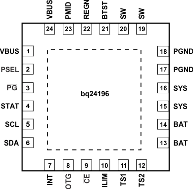
Pin Functions
| PIN | TYPE | DESCRIPTION | |
|---|---|---|---|
| NAME | NUMBER | ||
| VBUS | 1,24 | P | Charger Input Voltage. The internal n-channel reverse block MOSFET (RBFET) is connected between VBUS and PMID with VBUS on source. Place a 1-µF ceramic capacitor from VBUS to PGND and place it as close as possible to IC. (Refer to Application Information Section for details) |
| PSEL | 2 | I Digital |
Power source selection input. High indicates a USB host source and Low indicates an adapter source. |
| PG | 3 | O Digital |
Open drain active low power good indicator. Connect to the pull up rail via 10-kΩ resistor. LOW indicates a good input source if the input voltage is between UVLO and ACOV, above SLEEP mode threshold, and current limit is above 30 mA. |
| STAT | 4 | O Digital |
Open drain charge status output to indicate various charger operation. Connect to the pull up rail via 10-kΩ. LOW indicates charge in progress. HIGH indicates charge complete or charge disabled. When any fault condition occurs, STAT pin blinks at 1 Hz. |
| SCL | 5 | I Digital |
I2C Interface clock. Connect SCL to the logic rail through a 10-kΩ resistor. |
| SDA | 6 | I/O Digital |
I2C Interface data. Connect SDA to the logic rail through a 10-kΩ resistor. |
| INT | 7 | O Digital |
Open-drain Interrupt Output. Connect the INT to a logic rail via 10-kΩ resistor. The INT pin sends active low, 256-us pulse to host to report charger device status and fault. |
| OTG | 8 | I Digital |
USB current limit selection pin during buck mode, and active high enable pin during boost mode. |
| In buck mode with USB host (PSEL=High), when OTG = High, IIN limit = 500 mA and when OTG = Low, IIN limit = 100 mA. | |||
| The boost mode is activated when the REG01[5:4] = 10 and OTG pin is High. | |||
| CE | 9 | I Digital |
Active low Charge Enable pin. Battery charging is enabled when REG01[5:4] = 01 and CE pin = Low. CE pin must be pulled high or low. |
| ILIM | 10 | I Analog |
ILIM pin sets the maximum input current limit by regulating the ILIM voltage at 1 V. A resistor is connected from ILIM pin to ground to set the maximum limit as IINMAX = (1V/RILIM) × 530. The actual input current limit is the lower one set by ILIM and by I2C REG00[2:0]. The minimum input current programmed on ILIM pin is 500 mA. |
| TS1 | 11 | I Analog |
Temperature qualification voltage input #1. Connect a negative temperature coefficient thermistor. Program temperature window with a resistor divider from REGN to TS1 to GND. Charge suspends when either TS pin is out of range. Recommend 103AT-2 thermistor. |
| TS2 | 12 | I Analog |
Temperature qualification voltage input #2. Connect a negative temperature coefficient thermistor. Program temperature window with a resistor divider from REGN to TS2 to GND. Charge suspends when either TS pin is out of range. Recommend 103AT-2 thermistor. TS1 and TS2 pin can be connected together for single thermistor application. |
| BAT | 13,14 | P | Battery connection point to the positive terminal of the battery pack. The internal BATFET is connected between BAT and SYS. Connect a 10 µF closely to the BAT pin. |
| SYS | 15,16 | P | System connection point. The internal BATFET is connected between BAT and SYS. When the battery falls below the minimum system voltage, switch-mode converter keeps SYS above the minimum system voltage. (Refer to Application Information Section for inductor and capacitor selection.) |
| PGND | 17,18 | P | Power ground connection for high-current power converter node. Internally, PGND is connected to the source of the n-channel LSFET. On PCB layout, connect directly to ground connection of input and output capacitors of the charger. A single point connection is recommended between power PGND and the analog GND near the IC PGND pin. |
| SW | 19,20 | O Analog |
Switching node connecting to output inductor. Internally SW is connected to the source of the n-channel HSFET and the drain of the n-channel LSFET. Connect the 0.047-µF bootstrap capacitor from SW to BTST. |
| BTST | 21 | P | PWM high side driver positive supply. Internally, the BTST is connected to the anode of the boost-strap diode. Connect the 0.047-µF bootstrap capacitor from SW to BTST. |
| REGN | 22 | P | PWM low side driver positive supply output. Internally, REGN is connected to the cathode of the boost-strap diode. Connect a 4.7-µF (10-V rating) ceramic capacitor from REGN to analog GND. The capacitor should be placed close to the IC. REGN also serves as bias rail of TS1 and TS2 pins. |
| PMID | 23 | O Analog |
Connected to the drain of the reverse blocking MOSFET and the drain of HSFET. Given the total input capacitance, connect a 1-µF capacitor on VBUS to PGND, and the rest all on PMID to PGND. (Refer to Application Information Section for details) |
| Thermal Pad | – | P | Exposed pad beneath the IC for heat dissipation. Always solder thermal pad to the board, and have vias on the thermal pad plane star-connecting to PGND and ground plane for high-current power converter. |
7 Specifications
7.1 Absolute Maximum Ratings(1)
over operating free-air temperature range (unless otherwise noted)| MIN | MAX | UNIT | ||
|---|---|---|---|---|
| Voltage range (with respect to GND) | VBUS | –2 | 22 | V |
| PMID | –0.3 | 22 | V | |
| STAT, PG | –0.3 | 20 | V | |
| BTST | –0.3 | 26 | V | |
| SW | –2 | 20 | V | |
| BAT, SYS (converter not switching) | –0.3 | 6 | V | |
| SDA, SCL, INT, OTG, ILIM, REGN, TS1, TS2, CE, PSEL | –0.3 | 7 | V | |
| BTST TO SW | –0.3 | –7 | V | |
| PGND to GND | –0.3 | –0.3 | V | |
| Output sink current | INT, STAT, PG | 6 | mA | |
| Junction temperature | –40°C | 150 | °C | |
| Storage temperature, Tstg | –65 | 150 | °C | |
7.2 ESD Ratings
| VALUE | UNIT | |||
|---|---|---|---|---|
| V(ESD) | Electrostatic discharge | Human body model (HBM), per ANSI/ESDA/JEDEC JS-001(1) | 1000 | V |
| Charged device model (CDM), per JEDEC specification JESD22-C101(2) | 250 | |||
7.3 Recommended Operating Conditions
| MIN | MAX | UNIT | ||
|---|---|---|---|---|
| VIN | Input voltage | 3.9 | 17(1) | V |
| IIN | Input current | 3 | A | |
| ISYS | Output current (SYS) | 2.5 | A | |
| VBAT | Battery voltage | 4.4 | V | |
| IBAT | Fast charging current | 2.5 | A | |
| Discharging current with internal MOSFET | 6 (continuous) 9 (peak) (up to 1 sec duration) |
A | ||
| TA | Operating free-air temperature range | –40 | 85 | °C |
7.4 Thermal Information
| THERMAL METRIC(1) | bq24196 | UNIT | |
|---|---|---|---|
| RGE (24 PIN) | |||
| RθJA | Junction-to-ambient thermal resistance | 32.2 | °C/W |
| RθJCtop | Junction-to-case (top) thermal resistance | 29.8 | |
| RθJB | Junction-to-board thermal resistance | 9.1 | |
| ψJT | Junction-to-top characterization parameter | 0.3 | |
| ψJB | Junction-to-board characterization parameter | 9.1 | |
| RθJCbot | Junction-to-case (bottom) thermal resistance | 2.2 | |
7.5 Electrical Characteristics
VVBUS_UVLOZ < VVBUS < VACOV and VVBUS > VBAT + VSLEEP, TJ = –40°C to 125°C and TJ = 25°C for typical values unless other noted.7.6 Typical Characteristics
Table 1. Table of Figures
| FIGURE NO. | |
|---|---|
| System Light Load Efficiency vs System Load Current | Figure 1 |
| SYS Voltage Regulation vs System Load | Figure 2 |
| Charging Efficiency vs Charging Current | Figure 3 |
| Boost Mode Efficiency vs VBUS Load Current | Figure 4 |
| Boost Mode VBUS Voltage Regulation vs VBUS Load Current | Figure 5 |
| SYS Voltage vs Temperature | Figure 6 |
| BAT Voltage vs Temperature | Figure 7 |
| Input Current Limit vs Temperature | Figure 8 |
| Charge Current vs Temperature | Figure 9 |


8 Detailed Description
8.1 Overview
The bq24196 is an I2C controlled power path management device and a single cell Li-Ion battery charger. It integrates the input reverse-blocking FET (RBFET, Q1), high-side switching FET (HSFET, Q2), low-side switching FET (LSFET, Q3), and BATFET (Q4) between system and battery. The device also integrates the bootstrap diode for the high-side gate drive.

8.3 Feature Description
8.3.1 Device Power Up
8.3.1.1 Power-On-Reset (POR)
The internal bias circuits are powered from the higher voltage of VBUS and BAT. When VBUS or VBAT rises above UVLOZ, the sleep comparator, battery depletion comparator and BATFET driver are active. I2C interface is ready for communication and all the registers are reset to default value. The host can access all the registers after POR.
8.3.1.2 Power Up from Battery without DC Source
If only battery is present and the voltage is above depletion threshold (VBAT_DEPL), the BATFET turns on and connects battery to system. The REGN LDO stays off to minimize the quiescent current. The low RDSON in BATFET and the low quiescent current on BAT minimize the conduction loss and maximize the battery run time. The device always monitors the discharge current through BATFET. When the system is overloaded or shorted, the device will immediately turn off BATFET and keep BATFET off until the input source plugs in again.
8.3.1.2.1 BATFET Turn Off
The BATFET can be forced off by the host through I2C REG07[5]. This bit allows the user to independently turn off the BATFET when the battery condition becomes abnormal during charging. When BATFET is off, there is no path to charge or discharge the battery.
When battery is not attached, the BATFET should be turned off by setting REG07[5] to 1 to disable charging and supplement mode.
8.3.1.2.2 Shipping Mode
When end equipment is assembled, the system is connected to battery through BATFET. There will be a small leakage current to discharge the battery even when the system is powered off. In order to extend the battery life during shipping and storage, the device can turn off BATFET so that the system voltage is zero to minimize the leakage.
In order to keep BATFET off during shipping mode, the host has to disable the watchdog timer (REG05[5:4] = 00) and disable BATFET (REG07[5] = 1) at the same time.
Once the BATFET is disabled, the BATFET can be turned on by plugging in adapter.
8.3.1.3 Power Up from DC Source
When the DC source plugs in, the bq24196 checks the input source voltage to turn on REGN LDO and all the bias circuits. It also checks the input current limit before starts the buck converter.
8.3.1.3.1 REGN LDO
The REGN LDO supplies internal bias circuits as well as the HSFET and LSFET gate drive. The LDO also provides bias rail to TS1/TS2 external resistors. The pull-up rail of STAT and PGcan be connected to REGN as well.
The REGN is enabled when all the conditions are valid.
- VBUS above UVLOZ
- VBUS above battery + VSLEEPZ in buck mode or VBUS below battery + VSLEEPZ in boost mode
- After typical 220ms delay (100ms minimum) is complete
If one of the above conditions is not valid, the device is in high impedance mode (HIZ) with REGN LDO off. The device draws less than 50 µA from VBUS during HIZ state. The battery powers up the system when the device is in HIZ.
8.3.1.3.2 Input Source Qualification
After REGN LDO powers up, the bq24196 checks the current capability of the input source. The input source has to meet the following requirements to start the buck converter.
- VBUS voltage below 18 V (not in ACOV)
- VBUS voltage above 3.8 V when pulling 30 mA (poor source detection)
Once the input source passes all the conditions above, the status register REG08[2] goes high and the PG pin goes low. An INT is asserted to the host.
If the device fails the poor source detection, it will repeat the detection every 2 seconds.
8.3.1.3.3 Input Current Limit Detection
The USB ports on personal computers are convenient charging source for portable devices (PDs). If the portable device is attached to a USB host, the USB specification requires the portable device to draw limited current (100 mA/500 mA in USB 2.0, and 150 mA/900 mA in USB 3.0). If the portable device is attached to a charging port, it is allowed to draw up to 1.5 A.
After the PG is LOW or REG08[2] goes HIGH, the charger device always runs input current limit detection when a DC source plugs in unless the charger is in HIZ during host mode.
The bq24196 sets input current limit through PSEL and OTG pins.
After the input current limit detection is done, the host can write to REG00[2:0] to change the input current limit.
8.3.1.3.4 PSEL/OTG Pins Set Input Current Limit
The bq24196 has PSEL. It directly takes the USB PHY device output to decide whether the input is USB host or charging port.
Table 2. bq24196 Input Current Limit Detection
| PSEL | OTG | INPUT CURRENT LIMIT | REG08[7:6] |
|---|---|---|---|
| HIGH | LOW | 100 mA | 01 |
| HIGH | HIGH | 500 mA | 01 |
| LOW | — | 3 A | 10 |
8.3.1.3.5 HIZ State wth 100mA USB Host
In battery charging spec, the good battery threshold is the minimum charge level of a battery to power up the portable device successfully. When the input source is 100-mA USB host, and the battery is above bat-good threshold (VBATGD), the device follows battery charging spec and enters high impedance state (HIZ). In HIZ state, the device is in the lowest quiescent state with REGN LDO and the bias circuits off. The charger device sets REG00[7] to 1, and the VBUS current during HIZ state will be less than 30 µA. The system is supplied by the battery.
Once the charger device enters HIZ state in host mode, it stays in HIZ until the host writes REG00[7] = 0. When the processor host wakes up, it is recommended to first check if the charger is in HIZ state.
In default mode, the charger IC will reset REG00[7] back to 0 when input source is removed. When another source plugs in, the charger IC will run detection again, and update the input current limit.
8.3.1.3.6 Force Input Current Limit Detection
The host can force the charger device to run input current limit detection by setting REG07[7] = 1. After the detection is complete, REG07[7] will return to 0 by itself.
8.3.1.4 Converter Power-Up
After the input current limit is set, the converter is enabled and the HSFET and LSFET start switching. If battery charging is disabled, BATFET turns off. Otherwise, BATFET stays on to charge the battery.
The bq24196 provides soft-start when ramp up the system rail. When the system rail is below 2.2 V, the input current limit is forced to 100 mA. After the system rises above 2.2 V, the charger device sets the input current limit set by the lower value between register and ILIM pin.
As a battery charger, the bq24196 deploys a 1.5-MHz step-down switching regulator. The fixed frequency oscillator keeps tight control of the switching frequency under all conditions of input voltage, battery voltage, charge current and temperature, simplifying output filter design.
A type III compensation network allows using ceramic capacitors at the output of the converter. An internal saw-tooth ramp is compared to the internal error control signal to vary the duty cycle of the converter. The ramp height is proportional to the PMID voltage to cancel out any loop gain variation due to a change in input voltage.
In order to improve light-load efficiency, the device switches to PFM control at light load when battery is below minimum system voltage setting or charging is disabled. During the PFM operation, the switching duty cycle is set by the ratio of SYS and VBUS.
8.3.1.5 Boost Mode Operation from Battery
The bq24196 supports boost converter operation to deliver power from the battery to other portable devices through USB port. The boost mode output current rating meets the USB On-The-Go 500-mA output requirement. The maximum output current is 1.3 A. The boost operation can be enabled if the following conditions are valid:
- BAT above BATLOWV threshold (VBATLOWV set by REG04[1])
- VBUS less than BAT+VSLEEP (in sleep mode)
- Boost mode operation is enabled (OTG pin HIGH and REG01[5:4] = 10)
- After 220-ms delay from boost mode enable
In boost mode, the bq24196 employs a 1.5-MHz step-up switching regulator. Similar to buck operation, the device switches from PWM operation to PFM operation at light load to improve efficiency.
During boost mode, the status register REG08[7:6] is set to 11, the VBUS output is 5 V and the output current can reach up to 500 mA or 1.3 A, selected via I2C (REG01[0]).
Any fault during boost operation, including VBUS over-voltage or over-current, sets the fault register REG09[6] to 1 and an INT is asserted.
8.3.2 Power Path Management
The bq24196 accommodates a wide range of input sources from USB, wall adapter, to car battery. The device provides automatic power path selection to supply the system (SYS) from input source (VBUS), battery (BAT), or both.
8.3.2.1 Narrow VDC Architecture
The device deploys Narrow VDC architecture (NVDC) with BATFET separating system from battery. The minimum system voltage is set by REG01[3:1]. Even with a fully depleted battery, the system is regulated above the minimum system voltage (default 3.5 V).
When the battery is below minimum system voltage setting, the BATFET operates in linear mode (LDO mode), and the system is 150 mV above the minimum system voltage setting. As the battery voltage rises above the minimum system voltage, BATFET is fully on and the voltage difference between the system and battery is the VDS of BATFET.
When the battery charging is disabled or terminated, the system is always regulated at 150 mV above the minimum system voltage setting. The status register REG08[0] goes high when the system is in minimum system voltage regulation.
 Figure 10. V(SYS) vs V(BAT)
8.3.2.2 Dynamic Power Management
To meet maximum current limit in USB spec and avoid over loading the adapter, the bq24196 features Dynamic Power Management (DPM), which continuously monitors the input current and input voltage.
When input source is over-loaded, either the current exceeds the input current limit (REG00[2:0]) or the voltage falls below the input voltage limit (REG00[6:3]). The device then reduces the charge current until the input current falls below the input current limit and the input voltage rises above the input voltage limit.
When the charge current is reduced to zero, but the input source is still overloaded, the system voltage starts to drop. Once the system voltage falls below the battery voltage, the device automatically enters the supplement mode where the BATFET turns on and battery starts discharging so that the system is supported from both the input source and battery.
During DPM mode (either VINDPM or IINDPM), the status register REG08[3] will go high.
Figure 11 shows the DPM response with 9-V/1.2-A adapter, 3.2-V battery, 2.8-A charge current and 3.4-V minimum system voltage setting.
 Figure 11. DPM Response
8.3.2.3 Supplement Mode
When the system voltage falls below the battery voltage, the BATFET turns on and the BATFET gate is regulated the gate drive of BATFET so that the minimum BATFET VDS stays at 30 mV when the current is low. This prevents oscillation from entering and exiting the supplement mode. As the discharge current increases, the BATFET gate is regulated with a higher voltage to reduce RDSON until the BATFET is in full conduction. At this point onwards, the BATFET VDS linearly increases with discharge current. Figure 12 shows the V-I curve of the BATFET gate regulation operation. BATFET turns off to exit supplement mode when the battery is below battery depletion threshold.
 Figure 12. BATFET V-I Curve
8.3.3 Battery Charging Management
The bq24196 charges 1-cell Li-Ion battery with up to 2.5A charge current for high capacity tablet battery. The 12-mΩ BATFET improves charging efficiency and minimizes the voltage drop during discharging.
8.3.3.1 Autonomous Charging Cycle
With battery charging enabled at POR (REG01[5:4] = 01), the bq24196 can complete a charging cycle without host involvement. The device default charging parameters are listed in .
Table 3. Charging Parameter Default Setting
| DEFAULT MODE | bq24196 |
|---|---|
| Charging voltage | 4.208 V |
| Charging current | 2.048 A |
| Pre-charge current | 256 mA |
| Termination current | 256 mA |
| Temperature profile | Hot/Cold |
| Safety timer | 8 hours |
A new charge cycle starts when the following conditions are valid:
- Converter starts
- Battery charging is enabled by I2C register bit (REG01[5:4]) = 01 and CE is low
- No thermistor fault on TS1 and TS2
- No safety timer fault
- BATFET is not forced to turn off (REG07[5])
The charger device automatically terminates the charging cycle when the charging current is below termination threshold and charge voltage is above recharge threshold. When a full battery voltage is discharged below recharge threshold (REG04[0]), the bq24196 automatically starts another charging cycle.
The STAT output indicates the charging status of charging (LOW), charging complete or charge disable (HIGH) or charging fault (Blinking). The status register REG08[5:4] indicates the different charging phases: 00-charging disable, 01-precharge, 10-fast charge (constant current) and constant voltage mode, 11-charging done. Once a charging cycle is complete, an INT is asserted to notify the host.
The host can always control the charging operation and optimize the charging parameters by writing to the registers through I2C.
8.3.3.2 Battery Charging Profile
The device charges the battery in three phases: preconditioning, constant current and constant voltage. At the beginning of a charging cycle, the device checks the battery voltage and applies current.
Table 4. Charging Current Setting
| VBAT | CHARGING CURRENT | REG DEFAULT SETTING | REG08[5:4] |
|---|---|---|---|
| < 2 V | 100 mA | – | 01 |
| 2 V - 3 V | REG03[7:4] | 256 mA | 01 |
| > 3 V | REG02[7:2] | 2048 mA | 10 |
If the charger device is in DPM regulation or thermal regulation during charging, the actual charging current will be less than the programmed value. In this case, termination is temporarily disabled and the charging safety timer is counted at half the clock rate.
 Figure 13. Battery Charging Profile
8.3.3.3 Thermistor Cold/Hot Temperature Window
The bq24196 continuously monitors battery temperature by measuring the voltage between the TS pins and ground, typically determined by a negative temperature coefficient thermistor and an external voltage divider. The device compares this voltage against its internal thresholds to determine if charging is allowed. To initiate a charge cycle, the battery temperature must be within the VLTF to VHTF thresholds. During the charge cycle the battery temperature must be within the VLTF to VTCO thresholds, else the device suspends charging and waits until the battery temperature is within the VLTF to VHTF range.
 Figure 14. TS Resistor Network
When the TS fault occurs, the fault register REG09[2:0] indicates the actual condition on each TS pin and an INT is asserted to the host. The STAT pin indicates the fault when charging is suspended.
 Figure 15. TS Pin Thermistor Sense Thresholds
Assuming a 103AT NTC thermistor is used on the battery pack, the value RT1 and RT2 can be determined by using the following equations:

Select 0°C to 45°C range for Li-ion or Li-polymer battery,
RTHCOLD = 27.28 kΩ
RTHHOT = 4.911 kΩ
RT1 = 5.52 kΩ
RT2 = 31.23 kΩ
8.3.3.4 Charging Termination
The bq24196 terminates a charge cycle when the battery voltage is above recharge threshold, and the current is below termination current. After the charging cycle is complete, the BATFET turns off. The converter keeps running to power the system, and BATFET can turn back on to engage supplement mode.
When termination occurs, the status register REG08[5:4] is 11, and an INT is asserted to the host. Termination is temporarily disabled if the charger device is in input current/voltage regulation or thermal regulation. Termination can be disabled by writing 0 to REG05[7].
8.3.3.4.1 Termination when REG02[0] = 1
When REG02[0] is HIGH to reduce the charging current by 80%, the charging current could be less than the termination current. The charger device termination function should be disabled. When the battery is charged to fully capacity, the host disables charging through CE pin or REG01[5:4].
8.3.3.4.2 Termination when REG05[6] = 1
Usually the STAT bit indicates charging complete when the charging current falls below termination threshold. Write REG05[6] = 1 to enable an early “charge done” indication on STAT pin. The STAT pin goes high when the charge current reduces below 800 mA. The charging cycle is still on-going until the current falls below the termination threshold.
8.3.3.5 Charging Safety Timer
The bq24196 has safety timer to prevent extended charging cycle due to abnormal battery conditions.
In default mode, the device keeps charging the battery with 5-hour fast charging safety timer regardless of REG05[2:1] default value. At the end of the 5 hours, the EN_HIZ (REG00[7]) is set to signal the buck converter stops and the system load is supplied by the battery. The EN_HIZ bit can be cleared to restart the buck converter.
In host mode, the device keeps charging the battery until the fast charging safety timer expired. The duration of safety timer can be set by the REG05[2:1] bits (default = 8 hours). At the end of safety timer, the EN_HIZ (REG00[7]) is cleared to signal the buck converter continues to operation to supply system load.
The safety timer is 1 hour when the battery is below BATLOWV threshold. The user can program fast charge safety timer through I2C (REG05[2:1]). When safety timer expires, the fault register REG09[5:4] goes 11 and an INT is asserted to the host. The safety timer feature can be disabled via I2C (REG05[3]).
The following actions restart the safety timer:
- At the beginning of a new charging cycle
- Toggle the CE pin HIGH to LOW to HIGH (charge enable)
- Write REG01[5:4] from 00 to 01 (charge enable)
- Write REG05[3] from 0 to 1 (safety timer enable)
During input voltage/current regulation or thermal regulation, or when FORCE_20PCT (REG02[0]) bit is set, the safety timer counts at half clock rate since the actual charge current is likely to be below the register setting. For example, if the charger is in input current regulation (IINDPM) throughout the whole charging cycle, and the safety time is set to 5 hours, the safety timer will expire in 10 hours. This feature can be disabled by writing 0 to REG07[6].
It is recommended to disable safety timer first by clearing REG05[3] bit before safety timer configuration is changed. The safety timer should be re-enabled by setting REG05[3] bit.
8.3.3.6 USB Timer when Charging from USB100mA Source
The total charging time in default mode from USB100-mA source is limited by a 45-min max timer. At the end of the timer, the device stops the converter and goes to HIZ.
8.3.4 Status Outputs (PG, STAT, and INT)
8.3.4.1 Power Good Indicator (PG)
In bq24196, PG goes LOW to indicate a good input source when:
- VBUS above UVLO
- VBUS above battery (not in sleep)
- VBUS below ACOV threshold
- VBUS above 3.8 V when 30-mA current is applied (not a poor source)
8.3.4.2 Charging Status Indicator (STAT)
The bq24196 indicates charging state on the open drain STAT pin. The STAT pin can drive LED as the application diagram shows.
Table 5. STAT Pin State
| CHARGING STATE | STAT |
|---|---|
| Charging in progress (including recharge) | LOW |
| Charging complete | HIGH |
| Sleep mode, charge disable | HIGH |
| Charge suspend (Input over-voltage, TS fault, timer fault, input or system over-voltage) | blinking at 1Hz |
8.3.4.3 Interrupt to Host (INT)
In some applications, the host does not always monitor the charger operation. The INT notifies the system on the device operation. The following events will generate 256-us INT pulse.
- USB/adapter source identified (through PSEL and OTG pins)
- Good input source detected
- VVBUS - VBAT > VSLEEPZ
- VVBUS > VACOV
- current limit above IBADSRC
- Input removed
- Charge Complete
- Any FAULT event in REG09
When a fault occurs, the charger device sends out INT and keeps the fault state in REG09 until the host reads the fault register. Before the host reads REG09 and all the faults are cleared, the charger device would not send any INT upon new faults. In order to read the current fault status, the host has to read REG09 two times consecutively. The 1st reads fault register status from the last read and the 2nd reads the current fault register status.
8.3.5 Protections
8.3.5.1 Input Current Limit on ILIM
For safe operation, the bq24196 has an additional hardware pin on ILIM to limit maximum input current on ILIM pin. The input maximum current is set by a resistor from ILIM pin to ground as:

The actual input current limit is the lower value between ILIM setting and register setting (REG00[2:0]). For example, if the register setting is 111 for 3 A, and ILIM has a 353-Ω resistor to ground for 1.5 A, the input current limit is 1.5 A. ILIM pin can be used to set the input current limit rather than the register settings.
The device regulates ILIM pin at 1 V. If ILIM voltage exceeds 1 V, the device enters input current regulation (Refer to Dynamic Power Path Management section).
The voltage on the ILIM pin is proportional to the input current. The ILIM pin can be used to monitor the input current per Equation 3:

For example, if the ILIM pin sets 2 A, and the ILIM voltage is 0.6 V, the actual input current is 1.2 A. If the ILIM pin is open, the input current is limited to zero since ILIM voltage floats above 1 V. If the ILIM pin is short, the input current limit is set by the register.
8.3.5.2 Thermal Regulation and Thermal Shutdown
The bq24196 monitors the internal junction temperature TJ to avoid overheat the chip and limits the IC surface temperature. When the internal junction temperature exceeds the preset limit (REG06[1:0]), the device lowers down the charge current. The wide thermal regulation range from 60°C to 120°C allows the user to optimize the system thermal performance.
During thermal regulation, the actual charging current is usually below the programmed battery charging current. Therefore, termination is disabled, the safety timer runs at half the clock rate, and the status register REG08[1] goes high.
Additionally, the device has thermal shutdown to turn off the converter. The fault register REG09[5:4] is 10 and an INT is asserted to the host.
8.3.5.3 Voltage and Current Monitoring in Buck Mode
The bq24196 closely monitor the input and system voltage, as well as HSFET and LSFET current for safe buck mode operation.
8.3.5.3.1 Input Over-Voltage (ACOV)
The maximum input voltage for buck mode operation is 18 V. If VBUS voltage exceeds 18 V, the device stops switching immediately. During input over voltage (ACOV), the fault register REG09[5:4] will be set to 01. An INT is asserted to the host.
8.3.5.3.2 System Over-Voltage Protection (SYSOVP)
The charger device monitors the voltage at SYS. When system over-voltage is detected, the converter is stopped to protect components connected to SYS from high voltage damage.
8.3.5.4 Voltage and Current Monitoring in Boost Mode
The bq24196 closely monitors the VBUS voltage, as well as HSFET and LSFET current to ensure safe boost mode operation.
8.3.5.4.1 VBUS Over-Voltage Protection
The boost mode regulated output is 5 V. When an adapter plugs in during boost mode, the VBUS voltage will rise above regulation target. Once the VBUS voltage exceeds 5.3 V, the bq24196 stops switching and the device exits boost mode. The fault register REG09[6] is set high to indicate fault in boost operation. An INT is asserted to the host.
8.3.5.5 Battery Protection
8.3.5.5.1 Battery Over-Current Protection (BATOVP)
The battery over-voltage limit is clamped at 4% above the battery regulation voltage. When battery over voltage occurs, the charger device immediately disables charge. The fault register REG09[5] goes high and an INT is asserted to the host.
8.3.5.5.2 Charging During Battery Short Protection
If the battery voltage falls below 2 V, the charge current is reduced to 100 mA for battery safety.
8.3.5.5.3 System Over-Current Protection
If the system is shorted or exceeds the over-current limit, the BATFET is latched off. DC source insertion on VBUS is required to reset the latch-off condition and turn on BATFET.
8.3.6 Serial Interface
The bq24196 uses I2C compatible interface for flexible charging parameter programming and instantaneous device status reporting. I2C is a bi-directional 2-wire serial interface developed by Philips Semiconductor (now NXP Semiconductors). Only two bus lines are required: a serial data line (SDA) and a serial clock line (SCL). Devices can be considered as masters or slaves when performing data transfers. A master is the device which initiates a data transfer on the bus and generates the clock signals to permit that transfer. At that time, any device addressed is considered a slave.
The device operates as a slave device with address 6BH, receiving control inputs from the master device like micro controller or a digital signal processor. The I2C interface supports both standard mode (up to 100 kbits), and fast mode (up to 400 kbits).
Both SDA and SCL are bi-directional lines, connecting to the positive supply voltage via a current source or pull-up resistor. When the bus is free, both lines are HIGH. The SDA and SCL pins are open drain.
8.3.6.1 Data Validity
The data on the SDA line must be stable during the HIGH period of the clock. The HIGH or LOW state of the data line can only change when the clock signal on the SCL line is LOW. One clock pulse is generated for each data bit transferred.
 Figure 16. Bit Transfer on the I2C Bus
8.3.6.2 START and STOP Conditions
All transactions begin with a START (S) and can be terminated by a STOP (P). A HIGH to LOW transition on the SDA line while SCl is HIGH defines a START condition. A LOW to HIGH transition on the SDA line when the SCL is HIGH defines a STOP condition.
START and STOP conditions are always generated by the master. The bus is considered busy after the START condition, and free after the STOP condition.
 Figure 17. START and STOP conditions
8.3.6.3 Byte Format
Every byte on the SDA line must be 8 bits long. The number of bytes to be transmitted per transfer is unrestricted. Each byte has to be followed by an Acknowledge bit. Data is transferred with the Most Significant Bit (MSB) first. If a slave cannot receive or transmit another complete byte of data until it has performed some other function, it can hold the clock line SCL low to force the master into a wait state (clock stretching). Data transfer then continues when the slave is ready for another byte of data and release the clock line SCL.
 Figure 18. Data Transfer on the I2C Bus
8.3.6.4 Acknowledge (ACK) and Not Acknowledge (NACK)
The acknowledge takes place after every byte. The acknowledge bit allows the receiver to signal the transmitter that the byte was successfully received and another byte may be sent. All clock pulses, including the acknowledge 9th clock pulse, are generated by the master.
The transmitter releases the SDA line during the acknowledge clock pulse so the receiver can pull the SDA line LOW and it remains stable LOW during the HIGH period of this clock pulse.
When SDA remains HIGH during the 9th clock pulse, this is the Not Acknowledge signal. The master can then generate either a STOP to abort the transfer or a repeated START to start a new transfer.
8.3.6.5 Slave Address and Data Direction Bit
After the START, a slave address is sent. This address is 7 bits long followed by the eighth bit as a data direction bit (bit R/W). A zero indicates a transmission (WRITE) and a one indicates a request for data (READ).
 Figure 19. Complete Data Transfer
8.3.6.5.1 Single Read and Write
 Figure 20. Single Write
 Figure 21. Single Read
If the register address is not defined, the charger IC send back NACK and go back to the idle state.
8.3.6.5.2 Multi-Read and Multi-Write
The charger device supports multi-read and multi-write on REG00 through REG08.
 Figure 22. Multi-Write
 Figure 23. Multi-Read
The fault register REG09 locks the previous fault and only clears it after the register is read. For example, if Charge Safety Timer Expiration fault occurs but recovers later, the fault register REG09 reports the fault when it is read the first time, but returns to normal when it is read the second time. To verify real time fault, the fault register REG09 should be read twice to get the real condition. In addition, the fault register REG09 does not support multi-read or multi-write.
8.4 Device Functional Modes
8.4.1 Host Mode and Default Mode
The bq24196 is a host controlled device, but it can operate in default mode without host management. In default mode, bq24196 can be used as an autonomous charger with no host or with host in sleep.
When the charger is in default mode, REG09[7] is HIGH. When the charger is in host mode, REG09[7] is LOW. After power-on-reset, the device starts in watchdog timer expiration state, or default mode. All the registers are in the default settings.
Any write command to bq24196 transitions the device from default mode to host mode. All the device parameters can be programmed by the host. To keep the device in host mode, the host has to reset the watchdog timer by writing 1 twice to REG01[6] before the watchdog timer expires (REG05[5:4]), or disable watchdog timer by setting REG05[5:4] = 00.
 Figure 24. Watchdog Timer Flow Chart
8.4.1.1 Plug in USB100mA Source with Good Battery
When the input source is detected as 100-mA USB host, and the battery voltage is above batgood threshold (VBATGD), the charger device enters HIZ state to meet the battery charging spec requirement.
If the charger device is in host mode, it will stay in HIZ state even after the USB100-mA source is removed, and the adapter plugs in. During the HIZ state, REG00[7] is set HIGH and the system load is supplied from battery. It is recommended that the processor host always checks if the charger IC is in HIZ state when it wakes up. The host can write REG00[7] to 0 to exit HIZ state.
If the charger is in default mode, when the DC source is removed, the charger device will get out of HIZ state automatically. When the input source plugs in again, the charger IC runs detection on the input source and update the input current limit.
8.4.1.2 USB Timer when Charging from USB 100-mA Source
The total charging time in default mode from USB 100-mA source is limited by a 45-min max timer. At the end of the timer, the device stops the converter and goes to HIZ.
8.5 Register Map
Table 6. Register Map
| REGISTER | REGISTER NAME | RESET |
|---|---|---|
| REG00 | Input Source Control Register | 00110000, or 30 |
| REG01 | Power-On Configuration Register | 00011011, or 1B |
| REG02 | Charge Current Control Register | 01100000, or 60 |
| REG03 | Pre-Charge/Termination Current Control Register | 00010001, or 11 |
| REG04 | Charge Voltage Control Register | 11001010, or CA |
| REG05 | Charge Termination/Timer Control Register | 10011010, or 9A |
| REG06 | Thermal Regulation Control Register | 00000011, or 03 |
| REG07 | Misc Operation Control Register | 01001011, or 4B |
| REG08 | System Status Register | — |
| REG09 | Fault Register | — |
| REG0A | Vender / Part / Revision Status Register | — |
8.5.1 I2C Registers
Address: 6BH. REG00-07 support Read and Write. REG08-0A are read only.
8.5.1.1 Input Source Control Register REG00 (reset = 00110000, or 30)
| 7 | 6 | 5 | 4 | 3 | 2 | 1 | 0 |
| EN_HIZ | VINDPM[3] | VINDPM[2] | VINDPM[1] | VINDPM[0] | IINLIM[2] | IINLIM[1] | IINLIM[0] |
| R/W | R/W | R/W | R/W | R/W | R/W | R/W | R/W |
| LEGEND: R/W = Read/Write; R = Read only; -n = value after reset |
Table 7. REG00 Input Source Control Register Description
| BIT | FIELD | TYPE | RESET | DESCRIPTION | |
|---|---|---|---|---|---|
| Bit 7 | EN_HIZ | R/W | 0 | 0 – Disable, 1 – Enable | Default: Disable (0) |
| Input Voltage Limit | |||||
| Bit 6 | VINDPM[3] | R/W | 0 | 640 mV | Offset 3.88 V, Range: 3.88 V to 5.08 V Default: 4.36 V (0110) |
| Bit 5 | VINDPM[2] | R/W | 1 | 320 mV | |
| Bit 4 | VINDPM[1] | R/W | 1 | 160 mV | |
| Bit 3 | VINDPM[0] | R/W | 0 | 80 mV | |
| Input Current Limit (Actual input current limit is the lower of I2C and ILIM) | |||||
| Bit 2 | IINLIM[2] | R/W | 0 | 000 – 100 mA, 001 – 150 mA, 010 – 500 mA, 011 – 900 mA, 100 – 1.2 A, 101 – 1.5 A, 110 – 2 A, 111 – 3 A |
Default SDP: 100 mA (000)(OTG pin = 0) or 500 mA (010) (OTG pin = 1) Default DCP/CDP: 3 A (111) |
| Bit 1 | IINLIM[1] | R/W | 0 | ||
| Bit 0 | IINLIM[0] | R/W | 0 | ||
8.5.1.2 Power-On Configuration Register REG01 (reset = 00011011, or 1B)
| 7 | 6 | 5 | 4 | 3 | 2 | 1 | 0 |
| Register Reset | I2C Watchdog Timer Reset | CHG_CONFIG[1] | CHG_CONFIG[0] | SYS_MIN[2] | SYS_MIN[1] | SYS_MIN[0] | BOOST_LIM |
| R/W | R/W | R/W | R/W | R/W | R/W | R/W | R/W |
| LEGEND: R/W = Read/Write; R = Read only; -n = value after reset |
Table 8. REG01 Power-On Configuration Register Description
| BIT | FIELD | TYPE | RESET | DESCRIPTION | NOTE |
|---|---|---|---|---|---|
| Bit 7 | Register Reset | R/W | 0 | 0 – Keep current register setting, 1 – Reset to default |
Default: Keep current register setting (0) Back to 0 after register reset |
| Bit 6 | I2C Watchdog Timer Reset | R/W | 0 | 0 – Normal ; 1 – Reset | Default: Normal (0) Back to 0 after timer reset |
| Charger Configuration | |||||
| Bit 5 | CHG_CONFIG[1] | R/W | 0 | 00 – Charge Disable, 01 – Charge Battery, 10/11 – OTG |
Default: Charge Battery (01) |
| Bit 4 | CHG_CONFIG[0] | R/W | 1 | ||
| Minimum System Voltage Limit | |||||
| Bit 3 | SYS_MIN[2] | R/W | 1 | 0.4 V | Offset: 3.0 V, Range 3.0 V to 3.7 V Default: 3.5 V (101) |
| Bit 2 | SYS_MIN[1] | R/W | 0 | 0.2 V | |
| Bit 1 | SYS_MIN[0] | R/W | 1 | 0.1 V | |
| Boost Mode Current Limit | |||||
| Bit 0 | BOOST_LIM | R/W | 1 | 0 – 500 mA, 1 – 1.3 A | Default: 1.3 A (1) |
8.5.1.3 Charge Current Control Register REG02 (reset = 01100000, or 60)
| 7 | 6 | 5 | 4 | 3 | 2 | 1 | 0 |
| ICHG[5] | ICHG[4] | ICHG[3] | ICHG[2] | ICHG[1] | ICHG[0] | Reserved | FORCE_20PCT |
| R/W | R/W | R/W | R/W | R/W | R/W | R/W | R/W |
| LEGEND: R/W = Read/Write; R = Read only; -n = value after reset |
Table 9. REG02 Charge Current Control Register Description
8.5.1.4 Pre-Charge/Termination Current Control Register REG03 (reset = 00010001, or 11)
| 7 | 6 | 5 | 4 | 3 | 2 | 1 | 0 |
| IPRECHG[3] | IPRECHG[2] | IPRECHG[1] | IPRECHG[0] | ITERM[3] | ITERM[2] | ITERM[1] | ITERM[0] |
| R/W | R/W | R/W | R/W | R/W | R/W | R/W | R/W |
| LEGEND: R/W = Read/Write; R = Read only; -n = value after reset |
Table 10. REG03 Pre-Charge/Termination Current Control Register Description
| BIT | FIELD | TYPE | RESET | DESCRIPTION | NOTE |
|---|---|---|---|---|---|
| Pre-Charge Current Limit | |||||
| Bit 7 | IPRECHG[3] | R/W | 0 | 1024 mA | Offset: 128 mA, Range: 128 mA to 2048 mA Default: 256 mA (0001) |
| Bit 6 | IPRECHG[2] | R/W | 0 | 512 mA | |
| Bit 5 | IPRECHG[1] | R/W | 0 | 256 mA | |
| Bit 4 | IPRECHG[0] | R/W | 1 | 128 mA | |
| Termination Current Limit | |||||
| Bit 3 | ITERM[3] | R/W | 0 | 1024 mA | Offset: 128 mA Range: 128 mA to 2048 mA Default: 256 mA (0001) |
| Bit 2 | ITERM[2] | R/W | 0 | 512 mA | |
| Bit 1 | ITERM[1] | R/W | 0 | 256 mA | |
| Bit 0 | ITERM[0] | R/W | 1 | 128 mA | |
8.5.1.5 Charge Voltage Control Register REG04 (reset = 11001010, or CA)
| 7 | 6 | 5 | 4 | 3 | 2 | 1 | 0 |
| VREG[5] | VREG[4] | VREG[3] | VREG[2] | VREG[1] | VREG[0] | BATLOWV | VRECHG |
| R/W | R/W | R/W | R/W | R/W | R/W | R/W | R/W |
| LEGEND: R/W = Read/Write; R = Read only; -n = value after reset |
Table 11. REG04 Charge Voltage Control Register Description
8.5.1.6 Charge Termination/Timer Control Register REG05 (reset = 10011010, or 9A)
| 7 | 6 | 5 | 4 | 3 | 2 | 1 | 0 |
| EN_TERM | TERM_STAT | WATCHDOG[1] | WATCHDOG[0] | EN_TIMER | CHG_TIMER[1] | CHG_TIMER[0] | Reserved |
| R/W | R/W | R/W | R/W | R/W | R/W | R/W | R/W |
| LEGEND: R/W = Read/Write; R = Read only; -n = value after reset |
Table 12. REG05 Charge Termination/Timer Control Register Description
| BIT | FIELD | TYPE | RESET | DESCRIPTION | NOTE |
|---|---|---|---|---|---|
| Charging Termination Enable | |||||
| Bit 7 | EN_TERM | R/W | 1 | 0 – Disable, 1 – Enable | Default: Enable termination (1) |
| Termination Indicator Threshold | |||||
| Bit 6 | TERM_STAT | R/W | 0 | 0 – Match ITERM, 1 – STAT pin high before actual termination when charge current below 800 mA |
Default Match ITERM (0) |
| I2C Watchdog Timer Setting | |||||
| Bit 5 | WATCHDOG[1] | R/W | 0 | 00 – Disable timer, 01 – 40 s, 10 – 80 s, 11 – 160 s | Default: 40 s (01) |
| Bit 4 | WATCHDOG[0] | R/W | 1 | ||
| Charging Safety Timer Enable | |||||
| Bit 3 | EN_TIMER | R/W | 1 | 0 – Disable, 1 – Enable | Default: Enable (1) |
| Fast Charge Timer Setting | |||||
| Bit 2 | CHG_TIMER[1] | R/W | 0 | 00 – 5 hrs, 01 – 8 hrs, 10 – 12 hrs, 11 – 20 hrs | Default: 8 hours (01) (See Charging Safety Timer for details) |
| Bit 1 | CHG_TIMER[0] | R/W | 1 | ||
| Bit 0 | Reserved | R/W | 0 | 0 - Reserved | Reserved. Must write "0" |
8.5.1.7 Thermal Regulation Control Register REG06 (reset = 00000011, or 03)
| 7 | 6 | 5 | 4 | 3 | 2 | 1 | 0 |
| Reserved | Reserved | Reserved | Reserved | Reserved | Reserved | TREG[1] | TREG[0] |
| R/W | R/W | R/W | R/W | R/W | R/W | R/W | R/W |
| LEGEND: R/W = Read/Write; R = Read only; -n = value after reset |
Table 13. REG06 Thermal Regulation Control Register Description
| BIT | FIELD | TYPE | RESET | DESCRIPTION | NOTE |
|---|---|---|---|---|---|
| Bit 7 | Reserved | R/W | 0 | 0 - Reserved | Reserved. Must write "0" |
| Bit 6 | Reserved | R/W | 0 | 0 - Reserved | Reserved. Must write "0" |
| Bit 5 | Reserved | R/W | 0 | 0 - Reserved | Reserved. Must write "0" |
| Bit 4 | Reserved | R/W | 0 | 0 - Reserved | Reserved. Must write "0" |
| Bit 3 | Reserved | R/W | 0 | 0 - Reserved | Reserved. Must write "0" |
| Bit 2 | Reserved | R/W | 0 | 0 - Reserved | Reserved. Must write "0" |
| Thermal Regulation Threshold | |||||
| Bit 1 | TREG[1] | R/W | 1 | 00 – 60°C, 01 – 80°C, 10 – 100°C, 11 – 120°C | Default: 120°C (11) |
| Bit 0 | TREG[0] | R/W | 1 | ||
8.5.1.8 Misc Operation Control Register REG07 (reset = 01001011, or 4B)
| 7 | 6 | 5 | 4 | 3 | 2 | 1 | 0 |
| DPDM_EN | TMR2X_EN | BATFET_Disable | Reserved | Reserved | Reserved | INT_MASK[1] | INT_MASK[0] |
| R/W | R/W | R/W | R/W | R/W | R/W | R/W | R/W |
| LEGEND: R/W = Read/Write; R = Read only; -n = value after reset |
Table 14. REG07 Misc Operation Control Register Description
| BIT | FIELD | TYPE | RESET | DESCRIPTION | NOTE |
|---|---|---|---|---|---|
| Set default input current limit from PSEL/OTG pins | |||||
| Bit 7 | DPDM_EN | R/W | 0 | 0 – Not in D+/D– detection; 1 – Force D+/D– detection |
Default: Not in D+/D– detection (0), Back to 0 after detection complete |
| Safety Timer Setting during Input DPM and Thermal Regulation | |||||
| Bit 6 | TMR2X_EN | R/W | 1 | 0 – Safety timer not slowed by 2X during input DPM or thermal regulation, 1 – Safety timer slowed by 2X during input DPM or thermal regulation |
Default: Safety timer slowed by 2X (1) |
| Force BATFET Off | |||||
| Bit 5 | BATFET_Disable | R/W | 0 | 0 – Allow Q4 turn on, 1 – Turn off Q4 | Default: Allow Q4 turn on(0) |
| Bit 4 | Reserved | R/W | 0 | 0 – Reserved | |
| Bit 3 | Reserved | R/W | 1 | 1 – Reserved | |
| Bit 2 | Reserved | R/W | 0 | 0 – Reserved | |
| Bit 1 | INT_MASK[1] | R/W | 1 | 0 – No INT during CHRG_FAULT, 1 – INT on CHRG_FAULT | Default: INT on CHRG_FAULT (1) |
| Bit 0 | INT_MASK[0] | R/W | 1 | 0 – No INT during BAT_FAULT, 1 – INT on BAT_FAULT | Default: INT on BAT_FAULT (1) |
8.5.1.9 System Status Register REG08
| 7 | 6 | 5 | 4 | 3 | 2 | 1 | 0 |
| VBUS_STAT[1] | VBUS_STAT[0] | CHRG_STAT[1] | CHRG_STAT[0] | DPM_STAT | PG_STAT | THERM_STAT | VSYS_STAT |
| R | R | R | R | R | R | R | R |
| LEGEND: R = Read only; -n = value after reset |
Table 15. REG08 System Status Register Description
| BIT | FIELD | TYPE | DESCRIPTION |
|---|---|---|---|
| Bit 7 | VBUS_STAT[1] | R | 00 – Unknown (no input, or DPDM detection incomplete), 01 – USB host, 10 – Adapter port, 11 – OTG |
| Bit 6 | VBUS_STAT[0] | R | |
| Bit 5 | CHRG_STAT[1] | R | 00 – Not Charging, 01 – Pre-charge (<VBATLOWV), 10 – Fast Charging, 11 – Charge Termination Done |
| Bit 4 | CHRG_STAT[0] | R | |
| Bit 3 | DPM_STAT | R | 0 – Not DPM, 1 – VINDPM or IINDPM |
| Bit 2 | PG_STAT | R | 0 – Not Power Good, 1 – Power Good |
| Bit 1 | THERM_STAT | R | 0 – Normal, 1 – In Thermal Regulation |
| Bit 0 | VSYS_STAT | R | 0 – Not in VSYSMIN regulation (BAT > VSYSMIN), 1 – In VSYSMIN regulation (BAT < VSYSMIN) |
8.5.1.10 Fault Register REG09
| 7 | 6 | 5 | 4 | 3 | 2 | 1 | 0 |
| WATCHDOG_ FAULT |
BOOST_ FAULT |
CHRG_FAULT[1] | CHRG_FAULT[0] | BAT_FAULT | NTC_FAULT[2] | NTC_FAULT[1] | NTC_FAULT[0] |
| R | R | R | R | R | R | R | R |
| LEGEND: R = Read only; -n = value after reset |
Table 16. REG09 Fault Register Description
| BIT | FIELD | TYPE | DESCRIPTION |
|---|---|---|---|
| Bit 7 | WATCHDOG_FAULT | R | 0 – Normal, 1- Watchdog timer expiration |
| Bit 6 | BOOST_FAULT | R | 0 – Normal, 1 – VBUS overloaded (OCP), or VBUS OVP in boost mode |
| Bit 5 | CHRG_FAULT[1] | R | 00 – Normal, 01 – Input fault (VBUS OVP or VBAT < VBUS < 3.8 V), 10 - Thermal shutdown, 11 – Charge Safety Timer Expiration |
| Bit 4 | CHRG_FAULT[0] | R | |
| Bit 3 | BAT_FAULT | R | 0 – Normal, 1 – BATOVP |
| Bit 2 | NTC_FAULT[2] | R | 000 – Normal, 101 – Cold, 110 – Hot |
| Bit 1 | NTC_FAULT[1] | R | |
| Bit 0 | NTC_FAULT[0] | R |
8.5.1.11 Vender / Part / Revision Status Register REG0A (reset = 00101011, or 2B)
| 7 | 6 | 5 | 4 | 3 | 2 | 1 | 0 |
| Reserved | Reserved | PN[2] | PN[1] | PN[0] | TS_PROFILE | DEV_REG[0] | DEV_REG[1] |
| R | R | R | R | R | R | R | R |
| LEGEND: R = Read only; -n = value after reset |
Table 17. REG0A Vender / Part / Revision Status Register Description
| BIT | FIELD | TYPE | RESET | DESCRIPTION |
|---|---|---|---|---|
| Bit 7 | Reserved | R | 0 | 0 - Reserved |
| Bit 6 | Reserved | R | 0 | 0 - Reserved |
| Device Configuration | ||||
| Bit 5 | PN[2] | R | 1 | 101 |
| Bit 4 | PN[1] | R | 0 | |
| Bit 3 | PN[0] | R | 1 | |
| Bit 2 | TS_PROFILE | R | 0 | 0 - Cold/Hot window |
| Bit 1 | DEV_REG[0] | R | 1 | 11 |
| Bit 0 | DEV_REG[1] | R | 1 | |
9 Application and Implementation
NOTE
Information in the following applications sections is not part of the TI component specification, and TI does not warrant its accuracy or completeness. TI’s customers are responsible for determining suitability of components for their purposes. Customers should validate and test their design implementation to confirm system functionality.
9.1 Application Information
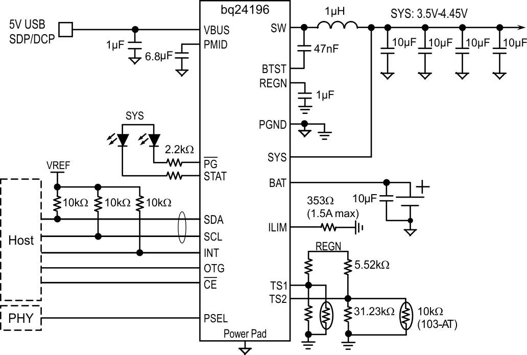
A typical application consists of the device configured as an I2C controlled power path management device and a single cell Li-Ion battery charger for single cell Li-Ion and Li-polymer batteries used in a wide range of tablets and other portable devices. It integrates an input reverse-blocking FET (RBFET, Q1), high-side switching FET (HSFET, Q2), low-side switching FET (LSFET, Q3), and BATFET (Q4) between the system and battery. The device also integrates a bootstrap diode for the high-side gate drive.
9.2 Typical Application

9.2.1 Design Requirements
Table 18. Design Requirements
| DESIGN PARAMETER | EXAMPLE VALUE |
|---|---|
| Input voltage | 3.9 V to 17 V |
| Input current limit | 3000 mA |
| Fast charge current | 2500 mA |
| Boost mode output current | 1.3 A |
9.2.2 Detailed Design Procedure
9.2.2.1 Inductor Selection
The bq24196 has 1.5-MHz switching frequency to allow the use of small inductor and capacitor values. The Inductor saturation current should be higher than the charging current (ICHG) plus half the ripple current (IRIPPLE):

The inductor ripple current depends on input voltage (VBUS), duty cycle (D = VBAT/VVBUS), switching frequency (fs) and inductance (L):

The maximum inductor ripple current happens with D = 0.5 or close to 0.5. Usually inductor ripple is designed in the range of (20 to 40%) maximum charging current as a trade-off between inductor size and efficiency for a practical design. Typical inductor value is 2.2 µH.
9.2.2.2 Input Capacitor
Input capacitor should have enough ripple current rating to absorb input switching ripple current. The worst case RMS ripple current is half of the charging current when duty cycle is 0.5. If the converter does not operate at 50% duty cycle, then the worst case capacitor RMS current ICIN occurs where the duty cycle is closest to 50% and can be estimated by the following equation:

For best performance, VBUS should be decouple to PGND with 1-μF capacitance. The remaining input capacitor should be place on PMID.
Low ESR ceramic capacitor such as X7R or X5R is preferred for input decoupling capacitor and should be placed to the drain of the high side MOSFET and source of the low side MOSFET as close as possible. Voltage rating of the capacitor must be higher than normal input voltage level. 25-V rating or higher capacitor is preferred for 15-V input voltage.
9.2.2.3 Output Capacitor
Output capacitor also should have enough ripple current rating to absorb output switching ripple current. The output capacitor RMS current ICOUT is given:

The output capacitor voltage ripple can be calculated as follows:

At certain input/output voltage and switching frequency, the voltage ripple can be reduced by increasing the output filter LC.
The charger device has internal loop compensator. To get good loop stability, the resonant frequency of the output inductor and output capacitor should be designed between 15 kHz and 25 kHz. With 2.2-µH inductor, the typical output capacitor value is 20 µF. The preferred ceramic capacitor is 6 V or higher rating, X7R or X5R.
9.2.3 Application Performance Plots

| VBAT 3.2 V | ||||

| VBUS 5 V | ||||

| VBUS 5 V, IIN 3 A, Charge Disable | ||

| VBUS 12 V, VBAT 3.8 V, ICHG 1.5 A | ||

| VBAT 3.8 V, ILOAD 1 A | ||

| VBUS 12 V | ||||

| VBUS 9 V, IIN 1.5 A, VBAT 3.8 V | ||

| VBUS 9 V, No Battery, ISYS 10 mA, Charge Disable | ||

| VBAT 3.8 V | ||||
10 Power Supply Recommendations
In order to provide an output voltage on SYS, the bq2419x require a power supply between 3.9 V and 17 V input with at least 100 mA current rating connected to VBUS; or, a single-cell Li-Ion battery with voltage > VBATUVLO connected to BAT. The source current rating needs to be at least 3 A in order for the buck converter of the charger to provide maximum output power to SYS.