SLUSBP6D september 2013 – april 2023 BQ24296 , BQ24297
PRODUCTION DATA
- 1 Features
- 2 Applications
- 3 Description
- 4 Revision History
- 5 Description (continued)
- 6 Device Comparison Table
- 7 Pin Configuration and Functions
- 8 Specifications
-
9 Detailed Description
- 9.1 Overview
- 9.2 Functional Block Diagram
- 9.3
Feature Description
- 9.3.1 Device Power Up
- 9.3.2 Power Path Management
- 9.3.3 Battery Charging Management
- 9.3.4 Status Outputs ( PG, STAT, and INT)
- 9.3.5 Protections
- 9.4 Device Functional Modes
- 9.5 Programming
- 9.6
Register Map
- 9.6.1
I2C Registers
- 9.6.1.1 Input Source Control Register REG00 [reset = 00110xxx, or 3x]
- 9.6.1.2 Power-On Configuration Register REG01 [reset = 00011011, or 0x1B]
- 9.6.1.3 Charge Current Control Register REG02 [reset = 01100000, or 60]
- 9.6.1.4 Pre-Charge/Termination Current Control Register REG03 [reset = 00010001, or 0x11]
- 9.6.1.5 Charge Voltage Control Register REG04 [reset = 10110010, or 0xB2]
- 9.6.1.6 Charge Termination/Timer Control Register REG05 [reset = 10011010, or 0x9A]
- 9.6.1.7 Boost Voltage/Thermal Regulation Control Register REG06 [reset = 01110011, or 0x73]
- 9.6.1.8 Misc Operation Control Register REG07 [reset = 01001011, or 4B]
- 9.6.1.9 System Status Register REG08
- 9.6.1.10 New Fault Register REG09
- 9.6.1.11 Vender / Part / Revision Status Register REG0A
- 9.6.1
I2C Registers
- 10Application and Implementation
- 11Power Supply Recommendations
- 12Layout
- 13Device and Documentation Support
- 14Mechanical, Packaging, and Orderable Information
Package Options
Mechanical Data (Package|Pins)
- RGE|24
Thermal pad, mechanical data (Package|Pins)
- RGE|24
Orderable Information
9.3.1.3.4 D+/D– Detection Sets Input Current Limit (BQ24297)
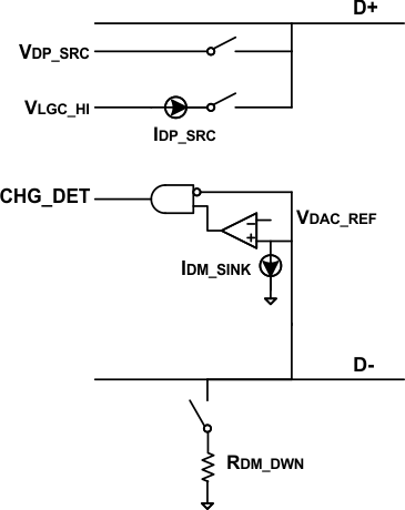
The BQ24297 contains a D+/D– based input source detection to program the input current limit. The D+/D- detection has three steps: data contact detect (DCD), primary detection, and non-standard adapter detection. When the charging source passes data contact detect, the device would proceed to run primary detection. Otherwise the charger would proceed to run non-standard adapter detection.
 Figure 9-2 USB D+/D- Detection
DCD (Data Contact Detection) uses a current source to detect when the D+/D– pins have made contact during an attach event. The protocol for data contact detect is as follows:
- Detect VBUS present and REG08[2] = 1 (power good)
- Turn on D+ IDP_SRC and the D– pull-down resistor RDM_DWN for 40 ms
- If the USB connector is properly attached, the D+ line goes from HIGH to LOW, wait up to 0.5 sec.
- Turn off IDP_SRC and disconnect RDM_DWN
The primary detection is used to distinguish between USB host (Standard Down Stream Port, or SDP) and different type of charging ports (Charging Down Stream Port, or CDP, and Dedicated Charging Port, or DCP). The protocol for primary detection is as follows:
- Turn on VDP_SRC on D+ and IDM_SINK on D– for 40 ms
- If PD is attached to a USB host (SDP), the D– is low. If PD is attached to a charging port (CDP or DCP), the D– is high
- Turn off VDP_SRC and IDM_SINK
Table 9-1 shows the input current limit setting after D+/D– detection.
| D+/D– DETECTION | OTG | INPUT CURRENT LIMIT | REG08[7:6] |
|---|---|---|---|
| 0.5 sec timer expired in DCD (D+/D- floating) | — | Proceed to non-standard adapter detection | 00 |
| USB host | LOW | 100 mA | 01 |
| USB host | HIGH | 500 mA | 01 |
| Charging port | — | 3 A | 10 |
When DCD 0.5 sec timer expires, the non-standard adapter detection is used to distinguish three different divider bias conditions on D+/D- pins. When non-standard adapter is detected, the input current limit (REG0[2:0]) is set based on the table shown below and REG08[7:6] is set to 10 (Adapter port). If non-standard adapter is not detected, REG08[7:6] is set to 00 (Unknown) and the input current limit is set in REG0[2:0] to 500 mA by default.
| NON-STANDARD ADAPTER | D+ THRESHOLD | D- THRESHOLD | INPUT CURRENT LIMIT |
|---|---|---|---|
| Divider 1 | Vadpt1_lo < VD+ < Vadpt1_hi For VBUS = 5 V, typical range 2.4 V < VD+ < 3.1 V | VD- < Vadpt1_lo or VD- > Vadpt1_hi For VBUS = 5 V, typical range VD- < 2.4 V or VD- > 3.1 V | 2.0A |
| Divider 2 | Vadpt2_lo < VD+ < Vadpt2_hi For VBUS = 5 V, typical range 0.85 V < VD+ < 1.5 V | NA | 2.0A |
| Divider 3 | VD+< Vadpt3_lo or VD+> Vadpt3_hi For VBUS = 5 V, typical range VD+ < 2.4 V or VD+ > 3.1 V | Vadpt3_lo < VD- < Vadpt3_hi For VBUS = 5 V, typical range 2.4 V < VD- < 3.1 V | 1A |
After D+/D- detection is completed with an input source already plugged in, the input current limit is not changed unless DPDM_EN (REG07[7]) bit is set to force detection.