SLUS912A August 2009 – August 2015
PRODUCTION DATA.
- 1 Features
- 2 Applications
- 3 Description
- 4 Revision History
- 5 Pin Configuration and Functions
- 6 Specifications
- 7 Detailed Description
- 8 Application and Implementation
- 9 Power Supply Recommendations
- 10Layout
- 11Device and Documentation Support
- 12Mechanical, Packaging, and Orderable Information
Package Options
Mechanical Data (Package|Pins)
- DSG|8
Thermal pad, mechanical data (Package|Pins)
- DSG|8
Orderable Information
8 Application and Implementation
NOTE
Information in the following applications sections is not part of the TI component specification, and TI does not warrant its accuracy or completeness. TI’s customers are responsible for determining suitability of components for their purposes. Customers should validate and test their design implementation to confirm system functionality.
8.1 Application Information
The bq24312 device protects against overvoltage, overcurrent, and battery overvoltage events that occur due to a faulty adapter or other input sources. If any of these faults occur, the bq24312 device isolates the downstream devices from the input source and alerts the host controller with the FAULT open-drain output.
8.1.1 Powering Accessories
In some applications, the equipment that the protection IC resides in may be required to provide power to an accessory (for example, a cellphone may power a headset or an external memory card) through the same connector pins that are used by the adapter for charging. Figure 10 and Figure 11 illustrate typical charging and accessory-powering scenarios:
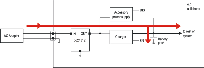 Figure 10. Charging - Red Arrows Show Direction of Current Flow
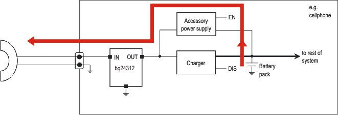 Figure 11. Powering an Accessory - Red Arrows Show Direction of Current Flow
In the second case, when power is being delivered to an accessory, the bq24312 device is required to support current flow from the OUT pin to the IN pin.
If VOUT > UVLO + 0.7 V, FET Q1 is turned on, and the reverse current does not flow through the diode but through Q1. Q1 will then remain ON as long as VOUT > UVLO – Vhys(UVLO) + RDS(on) × IACCESSORY. Within this voltage range, the reverse current capability is the same as the forward capability, 1.5 A. It should be noted that there is no overcurrent protection in this direction.
8.2 Typical Application
The typical values for an application are VOVP = 5.85 V, IOCP = 1000 mA, BVOVP = 4.35 V (Terminal numbers shown are for the 2 × 2 DSG package)
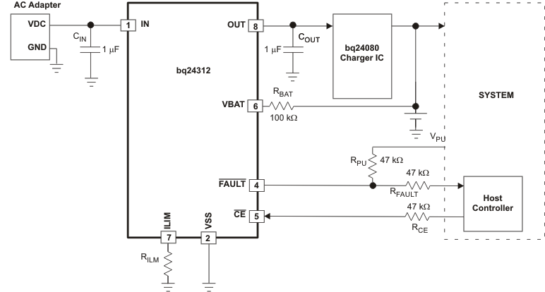 Figure 12. Typical Application Circuit
8.2.1 Design Requirements
For this design example, use the parameters listed in Table 1.
Table 1. Design Parameters
| DESIGN PARAMETER | EXAMPLE VALUE |
|---|---|
| Supply Voltage | 5 V |
| INILIM | 1 A |
8.2.2 Detailed Design Procedure
8.2.2.1 Selection Of RBAT
It is strongly recommended that the battery not be tied directly to the VBAT pin of the device, as under some failure modes of the device, the voltage at the IN pin may appear on the VBAT pin. This voltage can be as high as 30 V, and applying 30 V to the battery in case of the failure of the bq24312 device can be hazardous. Connecting the VBAT pin through RBAT prevents a large current from flowing into the battery in case of a failure of the device. In the interests of safety, RBAT should have a very high value. The problem with a large RBAT is that the voltage drop across this resistor because of the VBAT bias current IVBAT causes an error in the BVOVP threshold. This error is over and above the tolerance on the nominal 4.35 V BVOVP threshold.
Choosing RBAT in the range from 100 kΩ to 470 kΩ is a good compromise. In the case of an device failure, with RBAT equal to 100 kΩ, the maximum current flowing into the battery would be (30 V – 3 V) ÷ 100 kΩ = 246 μA, which is low enough to be absorbed by the bias currents of the system components. RBAT equal to 100 kΩ would result in a worst-case voltage drop of RBAT × IVBAT = 1 mV. This is negligible to compared to the internal tolerance of 50 mV on BVOVP threshold.
If the Bat-OVP function is not required, the VBAT pin should be connected to VSS.
8.2.2.2 Selection Of RCE, RFAULT, And RPU
The CE pin can be used to enable and disable the IC. If host control is not required, the CE pin can be tied to ground or left unconnected, permanently enabling the device.
In applications where external control is required, the CE pin can be controlled by a host processor. As in the case of the VBAT pin (see above), the CE pin should be connected to the host GPIO pin through as large a resistor as possible. The limitation on the resistor value is that the minimum VOH of the host GPIO pin less the drop across the resistor should be greater than VIH of the bq24312 device's CE pin. The drop across the resistor is given by RCE × IIH.
The FAULT pin is an open-drain output that goes low during OV, OC, battery-OV, and OT events. If the application does not require monitoring of the FAULT pin, it can be left unconnected. But if the FAULT pin has to be monitored, it should be pulled high externally through RPU, and connected to the host through RFAULT. RFAULT prevents damage to the host controller if the bq24312 device fails (see above). The resistors should be of high value, in practice values between 22 kΩ and 100 kΩ should be sufficient.
8.2.2.3 Selection Of Input And Output Bypass Capacitors
The input capacitor CIN in Figure 12 is for decoupling, and serves an important purpose. Whenever there is a step change downwards in the system load current, the inductance of the input cable causes the input voltage to spike up. CIN prevents the input voltage from overshooting to dangerous levels. It is strongly recommended that a ceramic capacitor of at least 1 μF be used at the input of the device. It should be located in close proximity to the IN pin.
COUT in Figure 12 is also important: If a very fast (< 1 μs rise time) overvoltage transient occurs at the input, the current that charges COUT causes the device’s current-limiting loop to kick in, reducing the gate-drive to FET Q1. This results in improved performance for input overvoltage protection. COUT should also be a ceramic capacitor of at least 1 μF, located close to the OUT pin. COUT also serves as the input decoupling capacitor for the charging circuit downstream of the protection IC.
8.2.3 Application Curves
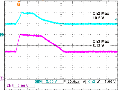
| VIN = 5 V to 10 V back to 5 V | ||
| tr = 10 μs | ||
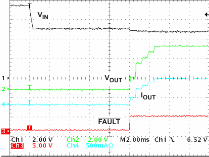
| VIN = 7.5 V to 5 V | ||
| tf = 400 μs |
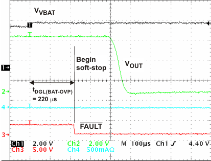
| VVBAT Steps from 4.2 V to 4.4 V | ||
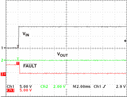
| VIN = 0 V to 9 V | ||
| tr = 50 μs |
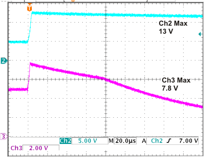
| VIN = 5 V to 12 V | ||
| tr = 4 μs |
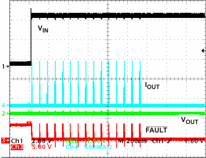
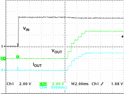
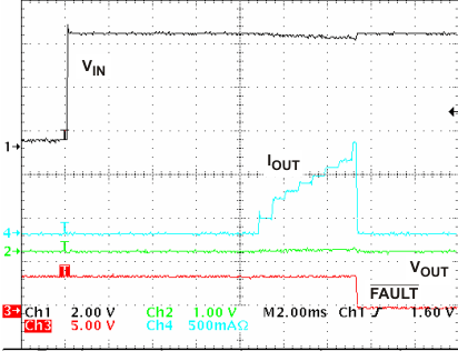
| OCP Counter Counts to 15 Before Switching OFF Device | ||
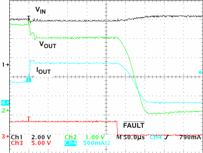
| ROUT Switches from 6.6 Ω to 3.3 Ω | ||
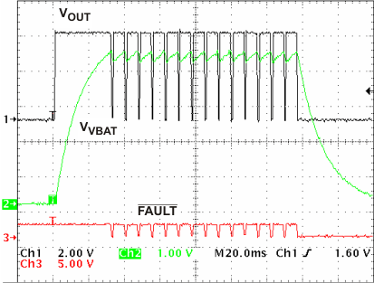
| VVBAT Cycles Between 4.1 V and 4.4 V | ||
