SLUS763D July 2007 – April 2016
PRODUCTION DATA.
- 1 Features
- 2 Applications
- 3 Description
- 4 Revision History
- 5 Pin Configuration and Functions
- 6 Specifications
- 7 Detailed Description
- 8 Applications and Implementation
- 9 Power Supply Recommendations
- 10Layout
- 11Device and Documentation Support
- 12Mechanical, Packaging, and Orderable Information
Package Options
Refer to the PDF data sheet for device specific package drawings
Mechanical Data (Package|Pins)
- DSJ|12
- DSG|8
Thermal pad, mechanical data (Package|Pins)
Orderable Information
9 Power Supply Recommendations
9.1 Powering Accessories
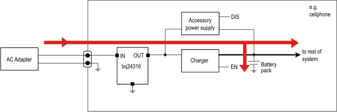
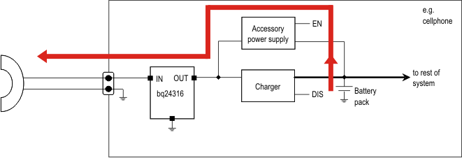
In some applications, the equipment that the protection IC resides in may be required to provide power to an accessory (for example, a cellphone may power a headset or an external memory card) through the same connector pins that are used by the adapter for charging. Figure 24 and Figure 25 illustrate typical charging and accessory-powering scenarios:
 Figure 24. Charging – the Red Arrows Show the Direction of Current Flow
 Figure 25. Powering an Accessory – the Red Arrows Show the Direction of Current Flow
In the second case, when power is being delivered to an accessory, the bq24314 and bq24316 devices are required to support current flow from the OUT pin to the IN pin.
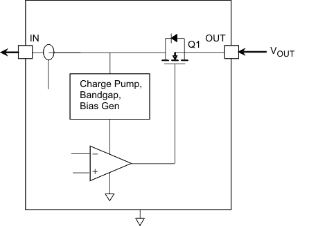
If VOUT > VUVLO + 0.7 V, FET Q1 is turned on, and the reverse current does not flow through the diode but through Q1 (see Figure 26). Q1 will then remain ON as long as VOUT > VUVLO – VHYS-UVLO + RDSON × IACCESSORY. Within this voltage range, the reverse current capability is the same as the forward capability, 1.5 A.
NOTE
There is no overcurrent protection in this direction.
 Figure 26. Powering an Accessory – Internal Power Path