SLUS891B February 2010 – November 2014
PRODUCTION DATA.
- 1 Features
- 2 Applications
- 3 Description
- 4 Revision History
- 5 Pin Configuration and Functions
- 6 Specifications
-
7 Detailed Description
- 7.1 Overview
- 7.2 Functional Block Diagram
- 7.3
Feature Description
- 7.3.1 Battery Voltage Regulation
- 7.3.2 Battery Current Regulation
- 7.3.3 Precharge
- 7.3.4 Charge Termination, Recharge, and Safety Timer
- 7.3.5 Power Up
- 7.3.6 Enable and Disable Charging
- 7.3.7 Automatic Internal Soft-Start Charger Current
- 7.3.8 Cycle-by-Cycle Charge Undercurrent Protection
- 7.3.9 Input Overvoltage Protection (ACOV)
- 7.3.10 Input Undervoltage Lock-Out (UVLO)
- 7.3.11 Battery Overvoltage Protection
- 7.3.12 Cycle-by-Cycle Charge Overcurrent Protection
- 7.3.13 Thermal Shutdown Protection
- 7.3.14 Temperature Qualification
- 7.3.15 Timer Fault Recovery
- 7.3.16 PG Output
- 7.3.17 CE (Charge Enable)
- 7.3.18 Inductor, Capacitor, and Sense Resistor Selection Guidelines
- 7.3.19 Charge Status Outputs
- 7.3.20 Battery Detection
- 7.4 Device Functional Modes
- 7.5 Application Information
- 7.6 Typical Application
- 8 Power Supply Recommendations
- 9 Layout
- 10Device and Documentation Support
- 11Mechanical, Packaging, and Orderable Information
Package Options
Mechanical Data (Package|Pins)
- RVA|16
Thermal pad, mechanical data (Package|Pins)
- RVA|16
Orderable Information
1 Features
- 1.2-MHz NMOS-NMOS Synchronous Buck Converter
- Stand-Alone Charger Support for Li-Ion or Li-Polymer
- 5-V – 28-V VCC Input Voltage Range and Supports 1S-6S Battery Cells
- Up to 10-A Charge Current and Adapter Current
- High-Accuracy Voltage and Current Regulation
- ±0.5% Charge-Voltage Accuracy
- ±3% Charge-Current Accuracy
- Integration
- Internal Loop Compensation
- Internal Soft Start
- Safety
- Input Overvoltage Protection
- Battery Thermistor Sense Hot/Cold Charge Suspend
- Battery Detection
- Built-In Safety Timer
- Charge Overcurrent Protection
- Battery Short Protection
- Battery Overvoltage Protection
- Thermal Shutdown
- Status Outputs
- Adapter Present
- Charger Operation Status
- Charge Enable Pin
- 6-V Gate Drive for Synchronous Power Converter
- 30-ns Driver Dead-Time and 99.5% Max. Effective Duty Cycle
- 16-Pin 3.5-mm × 3.5-mm QFN package
- Energy Star Low Quiescent Current Iq
- < 15-μA Off-State Battery Discharge Current
- < 1.5-mA Off-State Input Quiescent Current
2 Applications
3 Description
The bq24600 is a highly integrated Li-ion or Li-polymer switch-mode battery-charge controller. It offers a constant-frequency synchronous PWM controller with high-accuracy charge current and voltage regulation, charge preconditioning, termination, and charge status monitoring,
The bq24600 charges the battery in three phases: preconditioning, constant current, and constant voltage. Charge is terminated when the current reaches a minimum level. An internal charge timer provides a safety backup. The bq24600 automatically restarts the charge cycle if the battery voltage falls below an internal threshold, and enters a low-quiescent-current sleep mode when the input voltage falls below the battery voltage.
Device Information(1)
| PART NUMBER | PACKAGE | BODY SIZE (NOM) |
|---|---|---|
| bq24600 | VQFN (16) | 3.50 mm x 3.50 mm |
- For all available packages, see the orderable addendum at the end of the datasheet.
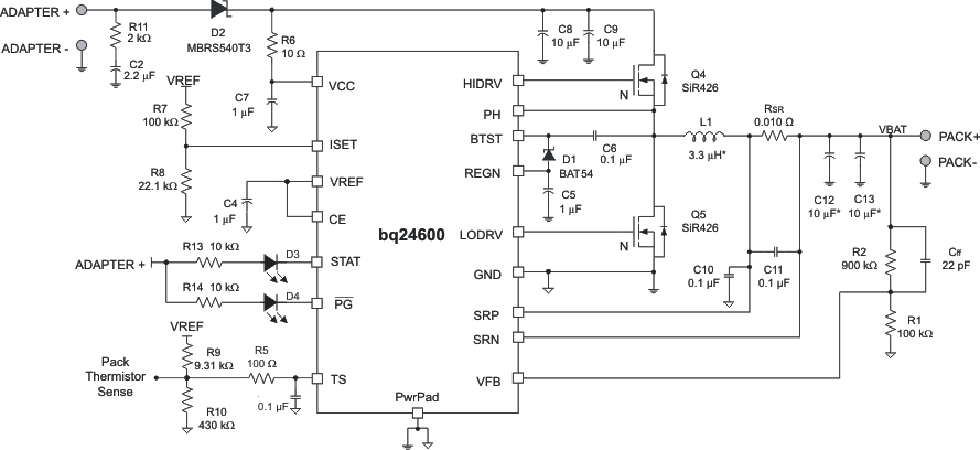
Simplified Schematic
4 Revision History
Changes from A Revision (October 2011) to B Revision
- Changed Added Handling Rating table, Feature Description section, Device Functional Modes, Application and Implementation section, Power Supply Recommendations section, Device and Documentation Go
- Changed feature text From: "Supports 1-6 Battery Cells" To: "Supports 1S-6S Battery Cells"Go
- Changed the Application list Go
- Deleted the Table of Graphs from the Typical Characteristics section Go
- Changed the Description of D3, D4 in Table 4 From: "LED diode, green, 2.1 V, 10 mΩ, Vishay-Dale, WSL2010R0100F" To:"LED diode, green, 2.1 V, 20 mA, LTST-C190GKT"Go
Changes from * Revision (February 2010) to A Revision
- Changed descriptions of PH and BTST pins in Pin Description tableGo
- Changed VHTF to VTCO in two places in Equation 5Go
- Changed Equation 15Go