SLUS892D December 2009 – December 2019 BQ24610 , BQ24617
PRODUCTION DATA.
- 1 Features
- 2 Applications
- 3 Description
- 4 Revision History
- 5 Description (continued)
- 6 Device Comparison Table
- 7 Pin Configuration and Functions
- 8 Specifications
-
9 Detailed Description
- 9.1 Overview
- 9.2 Functional Block Diagram
- 9.3
Feature Description
- 9.3.1 Battery Voltage Regulation
- 9.3.2 Battery Current Regulation
- 9.3.3 Input Adapter Current Regulation
- 9.3.4 Precharge
- 9.3.5 Charge Termination, Recharge, and Safety Timer
- 9.3.6 Power Up
- 9.3.7 Enable and Disable Charging
- 9.3.8 System Power Selector
- 9.3.9 Automatic Internal Soft-Start Charger Current
- 9.3.10 Converter Operation
- 9.3.11 Synchronous and Nonsynchronous Operation
- 9.3.12 Cycle-by-Cycle Charge Undercurrent Protection
- 9.3.13 Input Overvoltage Protection (ACOV)
- 9.3.14 Input Undervoltage Lockout (UVLO)
- 9.3.15 Battery Overvoltage Protection
- 9.3.16 Cycle-by-Cycle Charge Overcurrent Protection
- 9.3.17 Thermal Shutdown Protection
- 9.3.18 Temperature Qualification
- 9.3.19 Timer Fault Recovery
- 9.3.20 PG Output
- 9.3.21 CE (Charge Enable)
- 9.3.22 Charge Status Outputs
- 9.3.23 Battery Detection
- 9.4 Device Functional Modes
- 10Application and Implementation
- 11Power Supply Recommendations
- 12Layout
- 13Device and Documentation Support
- 14Mechanical, Packaging, and Orderable Information
Package Options
Mechanical Data (Package|Pins)
- RGE|24
Thermal pad, mechanical data (Package|Pins)
- RGE|24
Orderable Information
9.4 Device Functional Modes
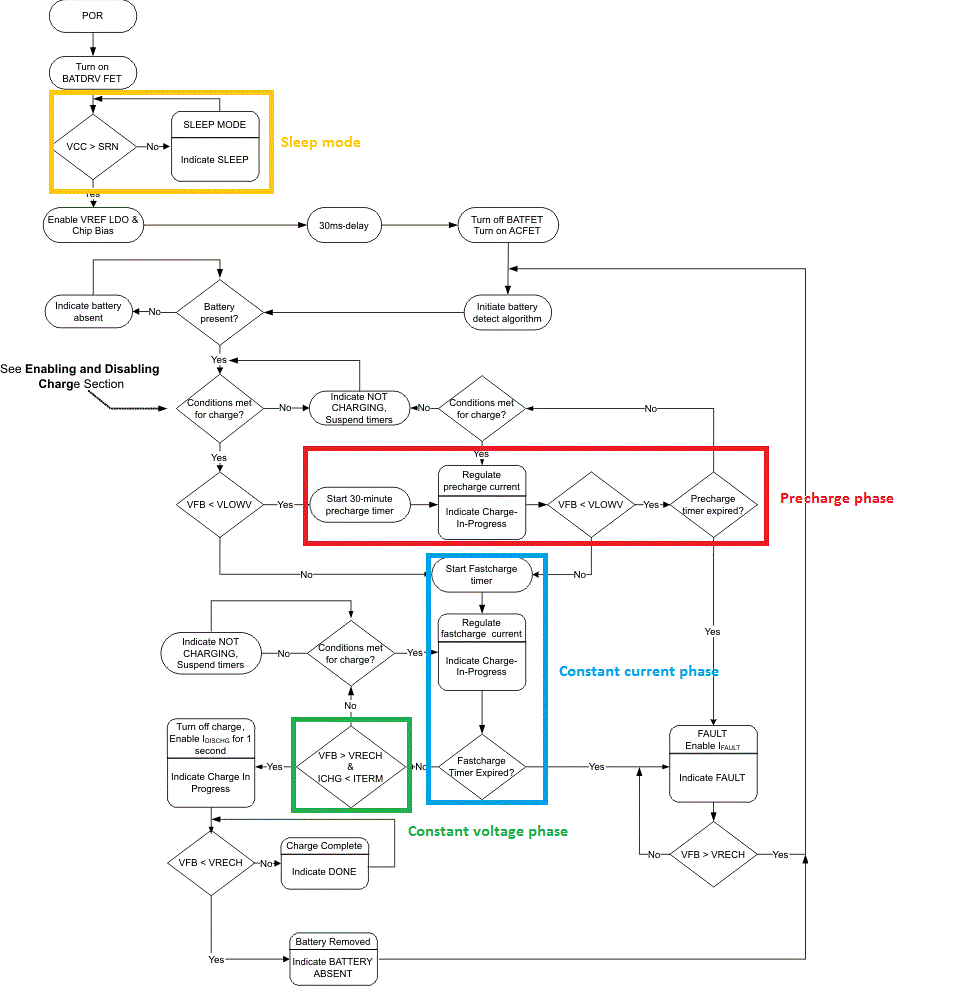
 Figure 19. Device Operation Flow Chart