SLUSAL0C September 2011 – January 2020 BQ24725A
PRODUCTION DATA.
- 1 Features
- 2 Applications
- 3 Description
- 4 Revision History
- 5 Pin Configuration and Functions
- 6 Specifications
- 7 Parameter Measurement Information
-
8 Detailed Description
- 8.1 Overview
- 8.2 Functional Block Diagram
- 8.3 Feature Description
- 8.4
Device Functional Modes
- 8.4.1 Adapter Detect and ACOK Output
- 8.4.2 Adapter Over Voltage (ACOVP)
- 8.4.3 System Power Selection
- 8.4.4 Battery LEARN Cycle
- 8.4.5 Enable and Disable Charging
- 8.4.6 Automatic Internal Soft-Start Charger Current
- 8.4.7 High Accuracy Current Sense Amplifier
- 8.4.8 Charge Timeout
- 8.4.9 Converter Operation
- 8.4.10 Continuous Conduction Mode (CCM)
- 8.4.11 Discontinuous Conduction Mode (DCM)
- 8.4.12 Input Over Current Protection (ACOC)
- 8.4.13 Charge Over Current Protection (CHGOCP)
- 8.4.14 Battery Over Voltage Protection (BATOVP)
- 8.4.15 Battery Shorted to Ground (BATLOWV)
- 8.4.16 Thermal Shutdown Protection (TSHUT)
- 8.4.17 EMI Switching Frequency Adjust
- 8.4.18 Inductor Short, MOSFET Short Protection
- 8.5 Register Maps
-
9 Application and Implementation
- 9.1 Application Information
- 9.2
Typical Applications
- 9.2.1
Typical System with Two NMOS Selector
- 9.2.1.1 Design Requirements
- 9.2.1.2
Detailed Design Procedure
- 9.2.1.2.1 Negative Output Voltage Protection
- 9.2.1.2.2 Reverse Input Voltage Protection
- 9.2.1.2.3 Reduce Battery Quiescent Current
- 9.2.1.2.4 Inductor Selection
- 9.2.1.2.5 Input Capacitor
- 9.2.1.2.6 Output Capacitor
- 9.2.1.2.7 Power MOSFETs Selection
- 9.2.1.2.8 Input Filter Design
- 9.2.1.2.9 BQ24725A Design Guideline
- 9.2.1.3 Application Curves
- 9.2.2 Simplified System without Power Path
- 9.2.1
Typical System with Two NMOS Selector
- 9.3 System Examples
- 10Power Supply Recommendations
- 11Layout
- 12Device and Documentation Support
- 13Mechanical, Packaging, and Orderable Information
Package Options
Mechanical Data (Package|Pins)
- RGR|20
Thermal pad, mechanical data (Package|Pins)
- RGR|20
Orderable Information
9.2.2 Simplified System without Power Path
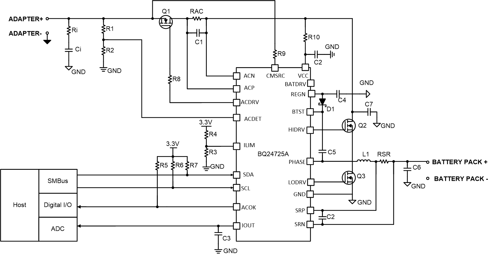
BQ24725A is SMBus controlled customizable charge controller, and Figure 25 simplified schematic shows if Power Path or ACFET is not required. To disable Power Path, BATDRV can be left floating. ACFET separates adapter from battery or system, and provides a limited di/dt when plugging in adapter by controlling the ACFET turn-on time. ACFET protects adapter when system or battery is shorted, however ACFET can be removed to simplify external components.

1. RBFET (Q1) provides negative input voltage protection and battery discharge protection when adapter is shorted to ground, and minimizes system power dissipation with its low RDS(on) compared to a Schottky diode. To simplify external components, RBFET can be removed, and ACDRV can be left floating. If RBFET is removed, it is recommended to include an external reverse blocking diode.
Figure 25. Simplified System Schematic without Power Path