SLUSAL0C September 2011 – January 2020 BQ24725A
PRODUCTION DATA.
- 1 Features
- 2 Applications
- 3 Description
- 4 Revision History
- 5 Pin Configuration and Functions
- 6 Specifications
- 7 Parameter Measurement Information
-
8 Detailed Description
- 8.1 Overview
- 8.2 Functional Block Diagram
- 8.3 Feature Description
- 8.4
Device Functional Modes
- 8.4.1 Adapter Detect and ACOK Output
- 8.4.2 Adapter Over Voltage (ACOVP)
- 8.4.3 System Power Selection
- 8.4.4 Battery LEARN Cycle
- 8.4.5 Enable and Disable Charging
- 8.4.6 Automatic Internal Soft-Start Charger Current
- 8.4.7 High Accuracy Current Sense Amplifier
- 8.4.8 Charge Timeout
- 8.4.9 Converter Operation
- 8.4.10 Continuous Conduction Mode (CCM)
- 8.4.11 Discontinuous Conduction Mode (DCM)
- 8.4.12 Input Over Current Protection (ACOC)
- 8.4.13 Charge Over Current Protection (CHGOCP)
- 8.4.14 Battery Over Voltage Protection (BATOVP)
- 8.4.15 Battery Shorted to Ground (BATLOWV)
- 8.4.16 Thermal Shutdown Protection (TSHUT)
- 8.4.17 EMI Switching Frequency Adjust
- 8.4.18 Inductor Short, MOSFET Short Protection
- 8.5 Register Maps
-
9 Application and Implementation
- 9.1 Application Information
- 9.2
Typical Applications
- 9.2.1
Typical System with Two NMOS Selector
- 9.2.1.1 Design Requirements
- 9.2.1.2
Detailed Design Procedure
- 9.2.1.2.1 Negative Output Voltage Protection
- 9.2.1.2.2 Reverse Input Voltage Protection
- 9.2.1.2.3 Reduce Battery Quiescent Current
- 9.2.1.2.4 Inductor Selection
- 9.2.1.2.5 Input Capacitor
- 9.2.1.2.6 Output Capacitor
- 9.2.1.2.7 Power MOSFETs Selection
- 9.2.1.2.8 Input Filter Design
- 9.2.1.2.9 BQ24725A Design Guideline
- 9.2.1.3 Application Curves
- 9.2.2 Simplified System without Power Path
- 9.2.1
Typical System with Two NMOS Selector
- 9.3 System Examples
- 10Power Supply Recommendations
- 11Layout
- 12Device and Documentation Support
- 13Mechanical, Packaging, and Orderable Information
Package Options
Mechanical Data (Package|Pins)
- RGR|20
Thermal pad, mechanical data (Package|Pins)
- RGR|20
Orderable Information
9.3 System Examples

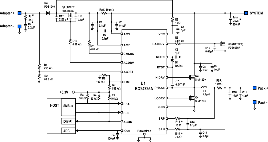
Fs = 750kHz, IADPT = 2.816A, ICHRG = 1.984A, ILIM = 2.54A, VCHRG = 12.592V, 65W adapter and 3S2P battery pack
Use 0Ω for better current sensing accuracy, use 10Ω/7.5Ω resistor for reversely battery connection protection. See application information about negative output voltage protection for hard shorts on battery to ground or battery reversely connection.
The total Csys is the lump sum of system capacitance. It is not required by charger IC. Use Ri and Ci for adapter hot plug in voltage spike damping. See application information about input filter design.
Figure 26. Typical System Schematic with One NMOS Selector and Schottky Diode 
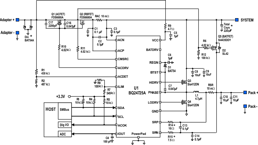
Fs = 750kHz, IADPT = 2.048A, ICHRG = 1.984A, ILIM = 2.54A, VCHRG = 4.200V, 12W adapter and 1S2P battery pack
Use 0Ω for better current sensing accuracy, use 10Ω/7.5Ω resistor for reversely battery connection protection. See application information about negative output voltage protection for hard shorts on battery to ground or battery reversely connection.
The total Csys is the lump sum of system capacitance. It is not required by charger IC. Use Din for reverse input protection. See application information about reverse input voltage protection. When using a different Q1 and Q2 that have a lower VGS(TH), a 500-kΩ resistor in parallel with C16 is required.
Figure 27. Typical System Schematic for 5V Input 1S Battery