SLUSBK6 July 2014
PRODUCTION DATA.
- 1 Features
- 2 Applications
- 3 Description
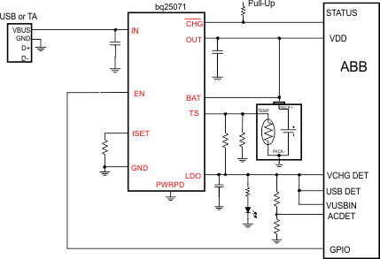
- 4 Application Schematic
- 5 Revision History
- 6 Device Comparison Table
- 7 Pin Configuration and Functions
- 8 Specifications
- 9 Detailed Description
- 10Application and Implementation
- 11Power Supply Recommendations
- 12Layout
- 13Device and Documentation Support
- 14Mechanical, Packaging, and Orderable Information
Package Options
Mechanical Data (Package|Pins)
- DQC|10
Thermal pad, mechanical data (Package|Pins)
Orderable Information
1 Features
- Single Cell LiFePO4 Charging Algorithm
- 30V Input Rating, With 10.5 V Overvoltage Protection (OVP)
- 50mA Integrated Low Dropout Linear Regulator (LDO)
- Programmable Charge Current Through ISET and EN Terminals
- 7% Charge Current Regulation Accuracy
- Thermal Regulation and Protection
- Soft-Start Feature to Reduce Inrush Current
- Battery NTC Monitoring
- Charging Status Indication
2 Applications
- Smart Phones
- Mobile Phones
- Portable Media Players
- Low Power Handheld Devices
3 Description
The bq25071 is a highly integrated, linear, LiFePO4 battery charger targeted at space-limited portable applications. It accepts power from either a USB port or AC adapter and charges a single-cell LiFePO4 battery with up to 1 A of charge current. The 30 V input rating with 10.5 V input overvoltage protection supports low-cost unregulated adapters.
The bq25071 has a single power output that simultaneously charges the battery and powers the system. The input current is programmable from 100 mA up to 1 A using the ISET input or configurable for USB500. There is also a 4.9 V ±10% 50 mA LDO integrated into the IC for supplying low power external circuitry.
The LiFePO4 charging algorithm removes the current taper typically seen as part of the constant voltage mode control used in Li-Ion battery charge cycles which reduces charge time significantly. Instead, the battery is fast charged to the overcharge voltage and then allowed to relax to a lower float charge voltage threshold. The charger integrates the power stage with the charge current and voltage sense to achieve a high level of accuracy in the current and voltage regulation loops. An internal control loop monitors the IC junction temperature through the charge cycle and reduces the charge current if an internal temperature threshold is exceeded.
Device Information(1)
| PART NUMBER | PACKAGE | BODY SIZE (NOM) |
|---|---|---|
| bq25071 | WSON (10) | 2.00mm x 3.00mm |
- For all available packages, see the orderable addendum at the end of the datasheet.
4 Application Schematic