SLUSDI4A October 2018 – April 2021 BQ25120F3A
PRODUCTION DATA
- 1 Features
- 2 Applications
- 3 Description
- 4 Revision History
- 5 Description (continued)
- 6 Device Comparison Table
- 7 Pin Configuration and Functions
- 8 Specifications
-
9 Detailed Description
- 9.1 Overview
- 9.2 Functional Block Diagram
- 9.3
Feature Description
- 9.3.1 Ship Mode
- 9.3.2 High Impedance Mode
- 9.3.3 Active Battery Only Connected
- 9.3.4 Voltage Based Battery Monitor
- 9.3.5 Sleep Mode
- 9.3.6 Input Voltage Based Dynamic Power Management (VIN(DPM))
- 9.3.7 Input Overvoltage Protection and Undervoltage Status Indication
- 9.3.8 Battery Charging Process and Charge Profile
- 9.3.9 Dynamic Power Path Management Mode
- 9.3.10 Battery Supplement Mode
- 9.3.11 Default Mode
- 9.3.12 Termination and Pre-Charge Current Programming by External Components (IPRETERM)
- 9.3.13 Input Current Limit Programming by External Components (ILIM)
- 9.3.14 Charge Current Programming by External Components (ISET)
- 9.3.15 Safety Timer and Watchdog Timer
- 9.3.16 External NTC Monitoring (TS)
- 9.3.17 Thermal Protection
- 9.3.18 Typical Application Power Dissipation
- 9.3.19 Status Indicators ( PG and INT)
- 9.3.20 Chip Disable ( CD)
- 9.3.21 Buck (PWM) Output
- 9.3.22 Load Switch / LDO Output and Control
- 9.3.23 Manual Reset Timer and Reset Output ( MR and RESET)
- 9.4 Device Functional Modes
- 9.5 Programming
- 9.6
Register Maps
- 9.6.1 Status and Ship Mode Control Register
- 9.6.2 Faults and Faults Mask Register
- 9.6.3 TS Control and Faults Masks Register
- 9.6.4 Fast Charge Control Register
- 9.6.5 Termination/Pre-Charge and I2C Address Register
- 9.6.6 Battery Voltage Control Register
- 9.6.7 SYS VOUT Control Register
- 9.6.8 Load Switch and LDO Control Register
- 9.6.9 Push-button Control Register
- 9.6.10 ILIM and Battery UVLO Control Register
- 9.6.11 Voltage Based Battery Monitor Register
- 9.6.12 VIN_DPM and Timers Register
- 10Application and Implementation
- 11Power Supply Recommendations
- 12Layout
- 13Device and Documentation Support
- 14Mechanical, Packaging, and Orderable Information
Package Options
Mechanical Data (Package|Pins)
- YFP|25
Thermal pad, mechanical data (Package|Pins)
Orderable Information
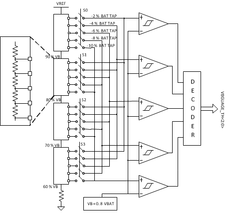
9.3.4 Voltage Based Battery Monitor
The device implements a simple voltage battery monitor which can be used to determine the depth of discharge. Prior to entering High-Z mode, the device will initiate a VBMON reading. The host can read the latched value for the no-load battery voltage, or initiate a reading using VBMON_READ to see the battery voltage under a known load. The register will be updated and can be read 2ms after a read is initiated. The VBMON voltage threshold is readable with 2% increments with ±1.5% accuracy between 60% and 100% of VBATREG using the VBMON_TH registers. Reading the value during charge is possible, but for the most accurate battery voltage indication, it is recommended to disable charge, initiate a read, and then re-enable charge.
A typical discharge profile for a Li-Ion battery is shown in Table 9-2. The specific battery to be used in the application should be fully characterized to determine the thresholds that will indicate the appropriate battery status to the user. Two typical examples are shown below, assuming the VBMON reading is taken with no load on the battery.
This function enables a simple 5-bar status indicator with the following typical performance with different VBATREG settings:
| VBATREG | BATTERY FULL | 95% to 65% REMAINING CAPACITY | 65% to 35% REMAINING CAPACITY | 35% to 5% REMAINING CAPACITY | BATTERY EMPTY |
|---|---|---|---|---|---|
| 4.35 V | VBMON > 90% | VBMON = 88% | VBMON = 86% | VBMON = 84% | VBMON < 82% |
| 4.2 V | VBMON > 98% | VBMON = 94% or 96% | VBMON = 90% or 92% | VBMON = 86% or 88% | VBMON < 84% |
 Figure 9-3 Voltage Battery Monitor