SLUSDI4A October 2018 – April 2021 BQ25120F3A
PRODUCTION DATA
- 1 Features
- 2 Applications
- 3 Description
- 4 Revision History
- 5 Description (continued)
- 6 Device Comparison Table
- 7 Pin Configuration and Functions
- 8 Specifications
-
9 Detailed Description
- 9.1 Overview
- 9.2 Functional Block Diagram
- 9.3
Feature Description
- 9.3.1 Ship Mode
- 9.3.2 High Impedance Mode
- 9.3.3 Active Battery Only Connected
- 9.3.4 Voltage Based Battery Monitor
- 9.3.5 Sleep Mode
- 9.3.6 Input Voltage Based Dynamic Power Management (VIN(DPM))
- 9.3.7 Input Overvoltage Protection and Undervoltage Status Indication
- 9.3.8 Battery Charging Process and Charge Profile
- 9.3.9 Dynamic Power Path Management Mode
- 9.3.10 Battery Supplement Mode
- 9.3.11 Default Mode
- 9.3.12 Termination and Pre-Charge Current Programming by External Components (IPRETERM)
- 9.3.13 Input Current Limit Programming by External Components (ILIM)
- 9.3.14 Charge Current Programming by External Components (ISET)
- 9.3.15 Safety Timer and Watchdog Timer
- 9.3.16 External NTC Monitoring (TS)
- 9.3.17 Thermal Protection
- 9.3.18 Typical Application Power Dissipation
- 9.3.19 Status Indicators ( PG and INT)
- 9.3.20 Chip Disable ( CD)
- 9.3.21 Buck (PWM) Output
- 9.3.22 Load Switch / LDO Output and Control
- 9.3.23 Manual Reset Timer and Reset Output ( MR and RESET)
- 9.4 Device Functional Modes
- 9.5 Programming
- 9.6
Register Maps
- 9.6.1 Status and Ship Mode Control Register
- 9.6.2 Faults and Faults Mask Register
- 9.6.3 TS Control and Faults Masks Register
- 9.6.4 Fast Charge Control Register
- 9.6.5 Termination/Pre-Charge and I2C Address Register
- 9.6.6 Battery Voltage Control Register
- 9.6.7 SYS VOUT Control Register
- 9.6.8 Load Switch and LDO Control Register
- 9.6.9 Push-button Control Register
- 9.6.10 ILIM and Battery UVLO Control Register
- 9.6.11 Voltage Based Battery Monitor Register
- 9.6.12 VIN_DPM and Timers Register
- 10Application and Implementation
- 11Power Supply Recommendations
- 12Layout
- 13Device and Documentation Support
- 14Mechanical, Packaging, and Orderable Information
Package Options
Mechanical Data (Package|Pins)
- YFP|25
Thermal pad, mechanical data (Package|Pins)
Orderable Information
10.2.3.5 Timing Waveforms Curves
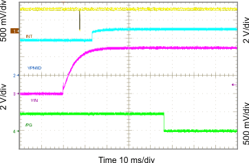 Figure 10-59 Show
PG and
INT Timing (VIN Insertion)
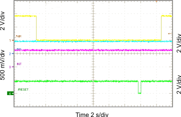
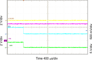 Figure 10-61 PG Functions as Shifted
MR Output
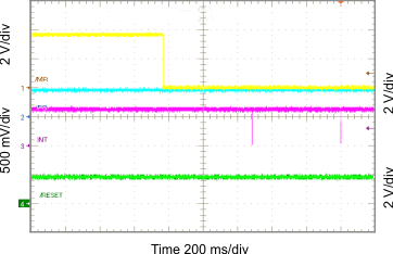
| Wake1 = 500 ms | Wake2 = 1 s |
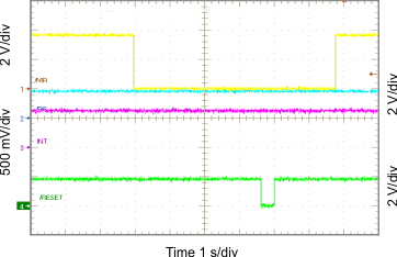
| RESET = 4 s |
| RESET = 14 s |
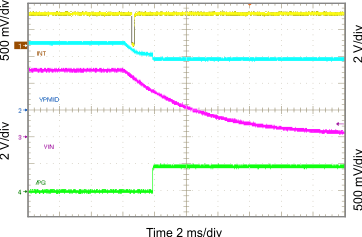 Figure 10-60 Show
PG and
INT Timing (VIN Removal)
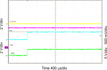 Figure 10-62 PG Functions as Shifted
MR Output
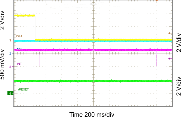
| Wake1 = 50 ms | Wake2 = 1.5 s |
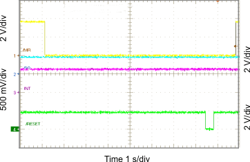
| RESET = 8 s |
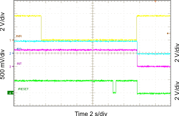 Figure 10-68 RESET Timing and Enter Ship Mode