SLUSEC5A december   2020  – august 2023 BQ25157

PRODUCTION DATA  

  1.   1
  2. Features
  3. Applications
  4. Description
  5. Revision History
  6. Description (continued)
  7. Device Key Default Settings
  8. Pin Configuration and Functions
  9. Specifications
    1. 8.1 Absolute Maximum Ratings
    2. 8.2 ESD Ratings
    3. 8.3 Recommended Operating Conditions
    4. 8.4 Thermal Information
    5. 8.5 Electrical Characteristics
    6. 8.6 Timing Requirements
    7. 8.7 Typical Characteristics
  10. Detailed Description
    1. 9.1 Overview
    2. 9.2 Functional Block Diagram
    3. 9.3 Feature Description
      1. 9.3.1  Linear Charger and Power Path
        1. 9.3.1.1 Battery Charging Process
          1. 9.3.1.1.1 Pre-Charge
          2. 9.3.1.1.2 Fast Charge
          3. 9.3.1.1.3 Pre-Charge to Fast Charge Transitions and Charge Current Ramping
          4. 9.3.1.1.4 Termination
        2. 9.3.1.2 JEITA and Battery Temperature Dependent Charging
        3. 9.3.1.3 Input Voltage Based Dynamic Power Management (VINDPM) and Dynamic Power Path Management (DPPM)
        4. 9.3.1.4 Battery Supplement Mode
      2. 9.3.2  Protection Mechanisms
        1. 9.3.2.1 Input Over-Voltage Protection
        2. 9.3.2.2 Safety Timer and I2C Watchdog Timer
        3. 9.3.2.3 Thermal Protection and Thermal Charge Current Foldback
        4. 9.3.2.4 Battery Short and Over Current Protection
        5. 9.3.2.5 PMID Short Circuit
      3. 9.3.3  ADC
        1. 9.3.3.1 ADC Operation in Active Battery Mode and Low Power Mode
        2. 9.3.3.2 ADC Operation When VIN Present
        3. 9.3.3.3 ADC Measurements
        4. 9.3.3.4 ADC Programmable Comparators
      4. 9.3.4  VDD LDO
      5. 9.3.5  Load Switch/LDO Output and Control
      6. 9.3.6  PMID Power Control
      7. 9.3.7  MR Wake and Reset Input
        1. 9.3.7.1 MR Wake or Short Button Press Functions
        2. 9.3.7.2 MR Reset or Long Button Press Functions
      8. 9.3.8  14-Second Watchdog for HW Reset
      9. 9.3.9  Faults Conditions and Interrupts ( INT)
        1. 9.3.9.1 Flags and Fault Condition Response
      10. 9.3.10 Power Good ( PG) Pin
      11. 9.3.11 External NTC Monitoring (TS)
        1. 9.3.11.1 TS Thresholds
      12. 9.3.12 External NTC Monitoring (ADCIN)
      13. 9.3.13 I2C Interface
        1. 9.3.13.1 F/S Mode Protocol
    4. 9.4 Device Functional Modes
      1. 9.4.1 Ship Mode
      2. 9.4.2 Low Power
      3. 9.4.3 Active Battery
      4. 9.4.4 Charger/Adapter Mode
      5. 9.4.5 Power-Up/Down Sequencing
    5. 9.5 Register Map
      1. 9.5.1 I2C Registers
  11. 10Application and Implementation
    1. 10.1 Application Information
    2. 10.2 Typical Application
      1. 10.2.1 Design Requirements
      2. 10.2.2 Detailed Design Procedure
        1. 10.2.2.1 Input (IN/PMID) Capacitors
        2. 10.2.2.2 VDD, LDO Input and Output Capacitors
        3. 10.2.2.3 TS
        4. 10.2.2.4 Recommended Passive Components
      3. 10.2.3 Application Curves
  12. 11Power Supply Recommendations
  13. 12Layout
    1. 12.1 Layout Guidelines
    2. 12.2 Layout Example
  14. 13Device and Documentation Support
    1. 13.1 Device Support
      1. 13.1.1 Third-Party Products Disclaimer
    2. 13.2 Documentation Support
      1. 13.2.1 Related Documentation
    3. 13.3 Receiving Notification of Documentation Updates
    4. 13.4 Support Resources
    5. 13.5 Electrostatic Discharge Caution
    6. 13.6 Trademarks
    7. 13.7 Glossary
  15. 14Mechanical, Packaging, and Orderable Information

Package Options

Mechanical Data (Package|Pins)
Thermal pad, mechanical data (Package|Pins)
Orderable Information

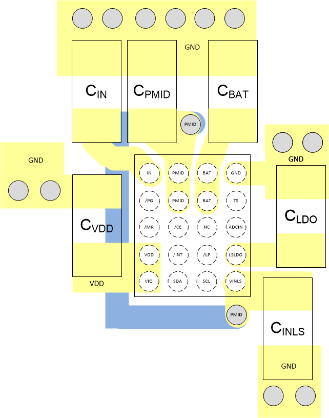
Layout Example

GUID-B64B41AD-CDAF-4AA0-9E44-E8127E27165C-low.gif Figure 12-1 Layout Example