SLUSF40 October   2024 BQ25190

PRODUCTION DATA  

  1.   1
  2. Features
  3. Applications
  4. Description
  5. Description (continued)
  6. Pin Configuration and Functions
  7. Specifications
    1. 6.1 Absolute Maximum Ratings
    2. 6.2 ESD Ratings
    3. 6.3 Thermal Information
    4. 6.4 Recommended Operating Conditions
    5. 6.5 Electrical Characteristics
    6. 6.6 Timing Requirements
    7. 6.7 Typical Characteristics
  8. Detailed Description
    1. 7.1 Overview
      1. 7.1.1 Battery Charging Process
        1. 7.1.1.1 Trickle Charge
        2. 7.1.1.2 Precharge
        3. 7.1.1.3 Fast Charge
        4. 7.1.1.4 Termination
    2. 7.2 Functional Block Diagram
    3. 7.3 Feature Description
      1. 7.3.1  Input Voltage Based Dynamic Power Management (VINDPM)
      2. 7.3.2  Dynamic Power Path Management Mode (DPPM)
      3. 7.3.3  Battery Supplement Mode
      4. 7.3.4  Sleep Mode
      5. 7.3.5  SYS Power Control
        1. 7.3.5.1 SYS Pulldown Control
      6. 7.3.6  SYS Regulation
      7. 7.3.7  ILIM Control
      8. 7.3.8  Protection Mechanisms
        1. 7.3.8.1  Input Overvoltage Protection
        2. 7.3.8.2  System Short Protection
        3. 7.3.8.3  Battery Depletion Protection
          1. 7.3.8.3.1 Battery Undervoltage Lockout
        4. 7.3.8.4  Battery Overcurrent Protection
        5. 7.3.8.5  Safety Timer and Watchdog Timer
        6. 7.3.8.6  Buck Overcurrent Protection
        7. 7.3.8.7  LDO Overcurrent Protection
        8. 7.3.8.8  Buck-Boost Overcurrent Protection
        9. 7.3.8.9  Buck-Boost Output Short-Circuit Protection
        10. 7.3.8.10 Buck/Buck-Boost/LDO Undervoltage Lockout
        11. 7.3.8.11 Sequence Undervoltage Lockout
        12. 7.3.8.12 Thermal Protection and Thermal Regulation
      9. 7.3.9  Integrated 12-Bit ADC for Monitoring
        1. 7.3.9.1 ADC Programmable Comparators
      10. 7.3.10 Pushbutton Wake and Reset Input
        1. 7.3.10.1 Pushbutton Short Button Press or Wake Functions
        2. 7.3.10.2 Pushbutton Long Button Press Functions
      11. 7.3.11 VIN Pulse Detection for Hardware Reset
      12. 7.3.12 15-Second VIN Watchdog for Hardware Reset
      13. 7.3.13 Hardware Reset
      14. 7.3.14 Software Reset
      15. 7.3.15 Interrupt to Host (INT)
      16. 7.3.16 External NTC Monitoring (TS)
        1. 7.3.16.1 TS Thresholds
      17. 7.3.17 Power Rail Power Sequence
        1. 7.3.17.1 Power-Up Sequence
        2. 7.3.17.2 Power-Down Sequence
      18. 7.3.18 Integrated Buck Converter (Buck)
      19. 7.3.19 Integrated Buck-Boost Converter (Buck-boost)
      20. 7.3.20 Integrated LDOs (LDO1/LDO2)
      21. 7.3.21 Multi-Function GPIOs
        1. 7.3.21.1 GPIO1 Functions
        2. 7.3.21.2 GPIO2 Functions
        3. 7.3.21.3 GPIO3 Functions
        4. 7.3.21.4 GPIO4 Functions
    4. 7.4 Device Functional Modes
      1. 7.4.1 Ship Mode
        1. 7.4.1.1 LDO1-ON Ship Mode
      2. 7.4.2 Battery Mode
      3. 7.4.3 Adapter Mode
    5. 7.5 Programming
      1. 7.5.1 Serial Interface
        1. 7.5.1.1 Data Validity
        2. 7.5.1.2 START and STOP Conditions
        3. 7.5.1.3 Byte Format
        4. 7.5.1.4 Acknowledge (ACK) and Not Acknowledge (NACK)
        5. 7.5.1.5 Target Address and Data Direction Bit
        6. 7.5.1.6 Single Write and Read
        7. 7.5.1.7 Multi-Write and Multi-Read
    6. 7.6 Register Maps
      1. 7.6.1 BQ25190 Registers
  9. Application and Implementation
    1. 8.1 Application Information
    2. 8.2 Typical Application
      1. 8.2.1 Design Requirements
      2. 8.2.2 Detailed Design Procedure
        1. 8.2.2.1 Input Capacitor Selection
        2. 8.2.2.2 Output Capacitor Selection
        3. 8.2.2.3 Inductor Selection
        4. 8.2.2.4 Recommended Passive Components
      3. 8.2.3 Application Performance Plots
  10. Power Supply Recommendations
  11. 10Layout
    1. 10.1 Layout Guidelines
    2. 10.2 Layout Example
  12. 11Device and Documentation Support
    1. 11.1 Third-Party Products Disclaimer
    2. 11.2 Receiving Notification of Documentation Updates
    3. 11.3 Support Resources
    4. 11.4 Trademarks
    5. 11.5 Electrostatic Discharge Caution
    6. 11.6 Glossary
  13. 12Revision History
  14. 13Mechanical, Packaging, and Orderable Information

Package Options

Refer to the PDF data sheet for device specific package drawings

Mechanical Data (Package|Pins)
  • YBG|30
Thermal pad, mechanical data (Package|Pins)
Orderable Information

Application Performance Plots

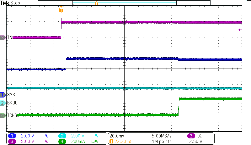
BQ25190 Adapter Plug-In with
                        Charge Enabled
VBAT = 3.2V ICHG = 200mA
Figure 8-2 Adapter Plug-In with Charge Enabled
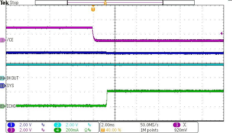
BQ25190 Charge Enable
VBAT = 3.2V ICHG = 200mA
Figure 8-4 Charge Enable
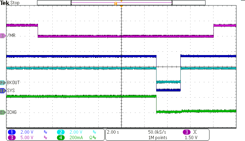
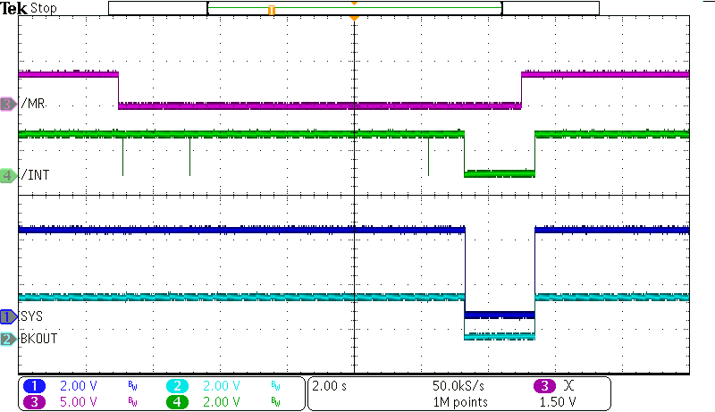
BQ25190 Hardware Reset by
                        Push-Button (MR) Press with Adapter
VBAT = 3.8V ICHG = 200mA
Figure 8-6 Hardware Reset by Push-Button (MR) Press with Adapter
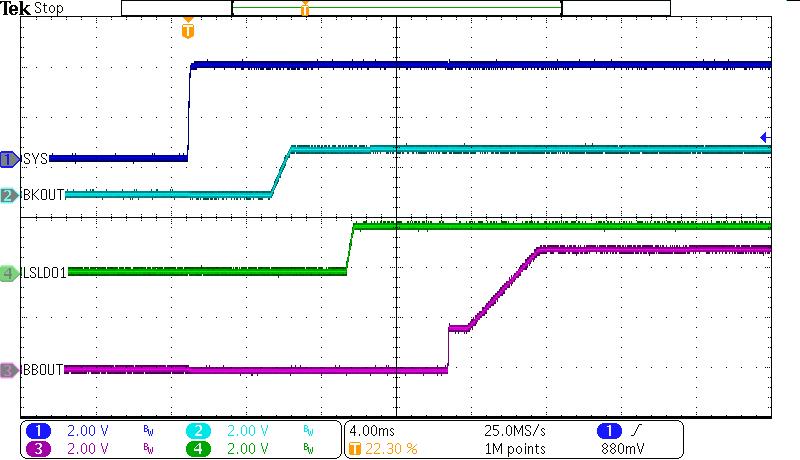
BQ25190 Power-Up Sequence During
                        Ship Mode Exit
VBAT = 3.8V VVINLS1 = VSYS
Figure 8-8 Power-Up Sequence During Ship Mode Exit
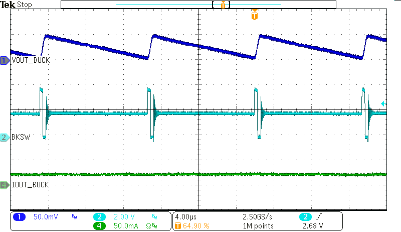
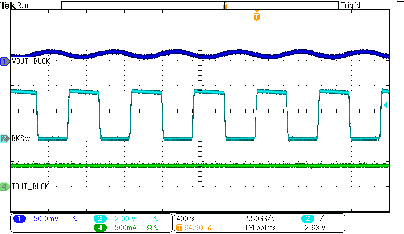
BQ25190 Buck Typical Operation
                        (Buck load = 20mA)
VBAT = VSYS = 3.8V VBKOUT = 1.8V
Figure 8-10 Buck Typical Operation (Buck load = 20mA)
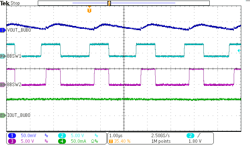
BQ25190 Buck-Boost Typical
                        Operation (Buck-boost load = 50mA)
VBAT = VSYS = 3.8V VBBOUT = 5V
Figure 8-12 Buck-Boost Typical Operation (Buck-boost load = 50mA)
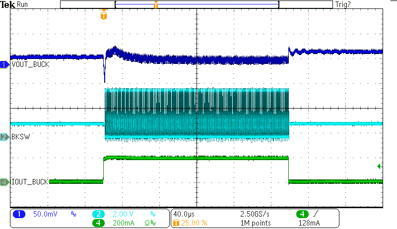
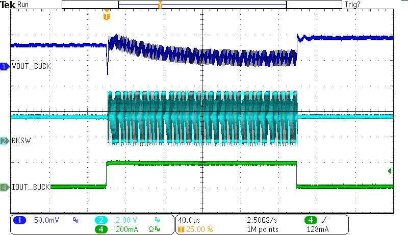
BQ25190 Buck Load Transient (Buck
                        load = 0 to 200mA)
VBAT = VSYS = 3.8V VBKOUT = 1V
Figure 8-14 Buck Load Transient (Buck load = 0 to 200mA)
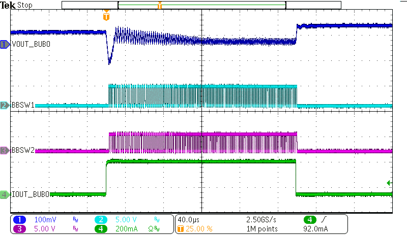
BQ25190 Buck-Boost Load Transient
                        (Buck-boost load = 0 to 250mA)
VBAT = VSYS = 3.8V VBBOUT = 3.3V
Figure 8-16 Buck-Boost Load Transient (Buck-boost load = 0 to 250mA)
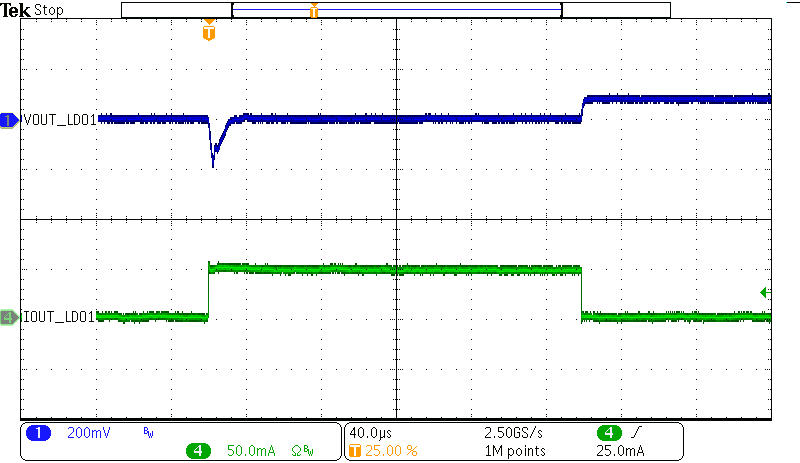
BQ25190 LDO1 Load Transient (LDO1
                        load = 0 to 50mA)
VBAT = VSYS = VVINLS1 = 3.8V VLSLDO1 = 1.8V
Figure 8-18 LDO1 Load Transient (LDO1 load = 0 to 50mA)
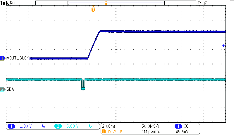
BQ25190 Buck Enable (No
                        load)
VBAT = VSYS = 3.8V VBKOUT = 1.8V
Figure 8-20 Buck Enable (No load)
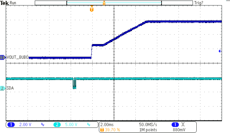
BQ25190 Buck-Boost Enable (No
                        load)
VBAT = VSYS = 3.8V VBBOUT = 5V
Figure 8-22 Buck-Boost Enable (No load)
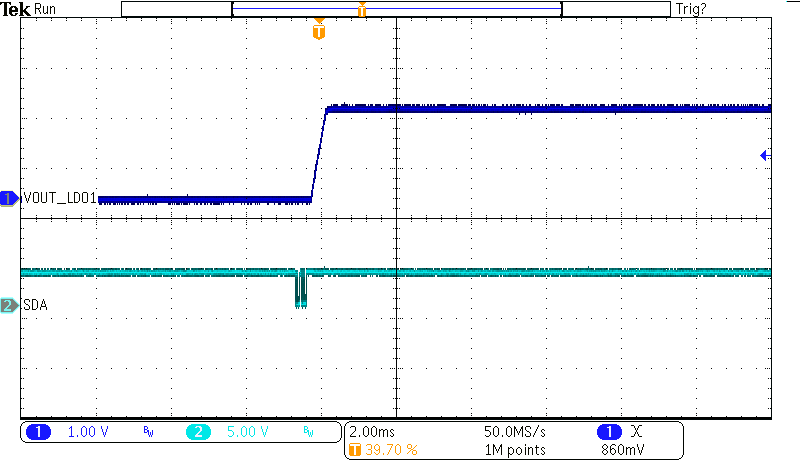
BQ25190 LDO1 Enable (No load)
VBAT = VSYS = VVINLS1 = 3.8V VLSLDO1 = 1.8V
Figure 8-24 LDO1 Enable (No load)
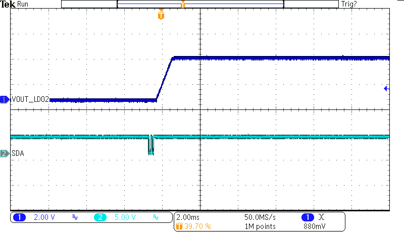
BQ25190 LDO2 Enable (No
                        load)
VBAT = VSYS = VVINLS2 = 3.8V VLSLDO2 = 3.3V
Figure 8-26 LDO2 Enable (No load)
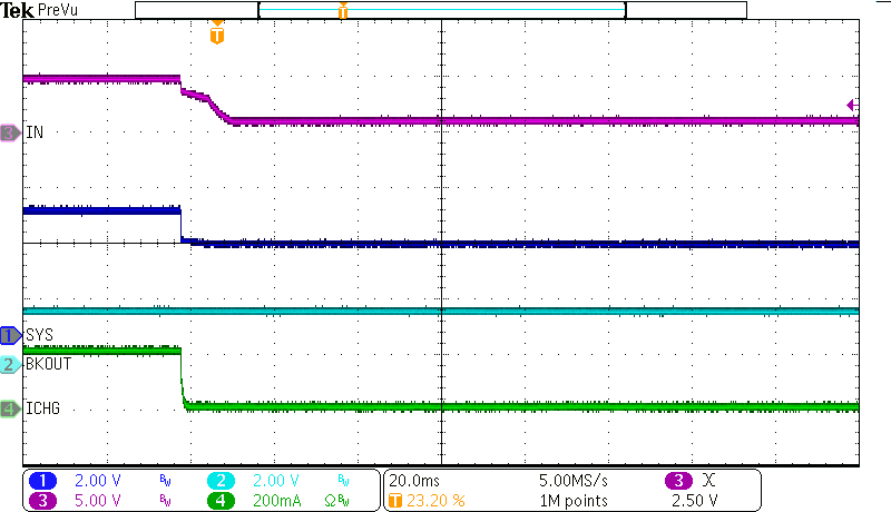
BQ25190 Adapter Unplug with Charge Enabled
VBAT = 3.2V ICHG = 200mA
Figure 8-3 Adapter Unplug with Charge Enabled
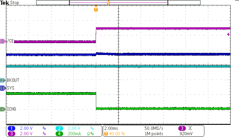
BQ25190 Charge Disable
VBAT = 3.2V ICHG = 200mA
Figure 8-5 Charge Disable
BQ25190 Hardware Reset by
                        Push-Button (MR) Press without Adapter
VBAT = 3.8V
Figure 8-7 Hardware Reset by Push-Button (MR) Press without Adapter
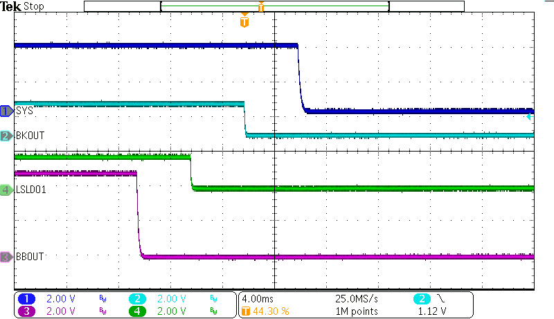
BQ25190 Power-Down Sequence
                        (default) During Ship Mode Entry
VBAT = 3.8V
Figure 8-9 Power-Down Sequence (default) During Ship Mode Entry
BQ25190 Buck Typical Operation
                        (Buck load = 400mA)
VBAT = VSYS = 3.8V VBKOUT = 1.8V
Figure 8-11 Buck Typical Operation (Buck load = 400mA)
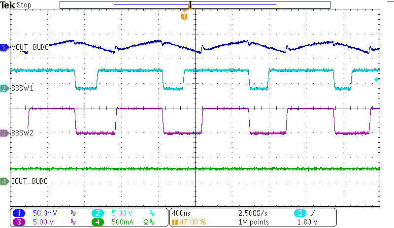
BQ25190 Buck-Boost Typical
                        Operation (Buck-boost load = 250mA)
VBAT = VSYS = 3.8V VBBOUT = 5V
Figure 8-13 Buck-Boost Typical Operation (Buck-boost load = 250mA)
BQ25190 Buck Load Transient (Buck
                        load = 0 to 200mA)
VBAT = VSYS = 3.8V VBKOUT = 1.8V
Figure 8-15 Buck Load Transient (Buck load = 0 to 200mA)
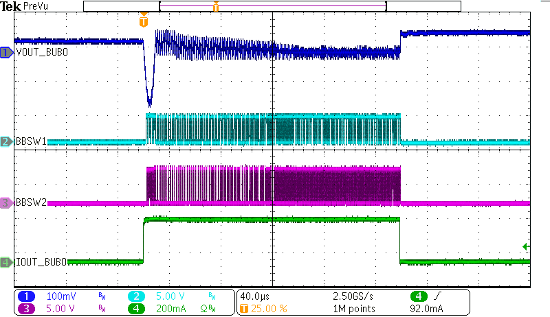
BQ25190 Buck-Boost Load Transient
                        (Buck-boost load = 0 to 250mA)
VBAT = VSYS = 3.8V VBBOUT = 5V
Figure 8-17 Buck-Boost Load Transient (Buck-boost load = 0 to 250mA)
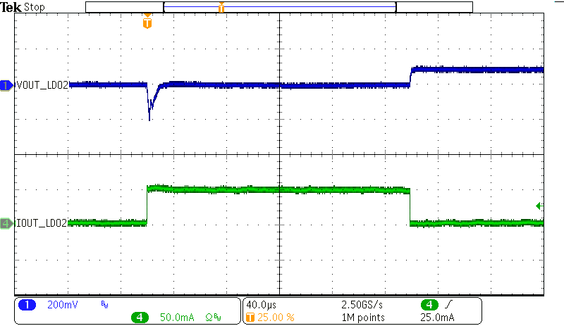
BQ25190 LDO2 Load Transient (LDO2
                        load = 0 to 50mA)
VBAT = VSYS = VVINLS2 = 3.8V VLSLDO2 = 3.3V
Figure 8-19 LDO2 Load Transient (LDO2 load = 0 to 50mA)
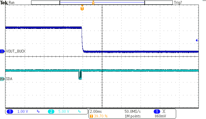
BQ25190 Buck Disable (No
                        load)
VBAT = VSYS = 3.8V VBKOUT = 1.8V
Figure 8-21 Buck Disable (No load)
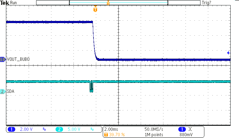
BQ25190 Buck-Boost Disable (No
                        load)
VBAT = VSYS = 3.8V VBBOUT = 5V
Figure 8-23 Buck-Boost Disable (No load)
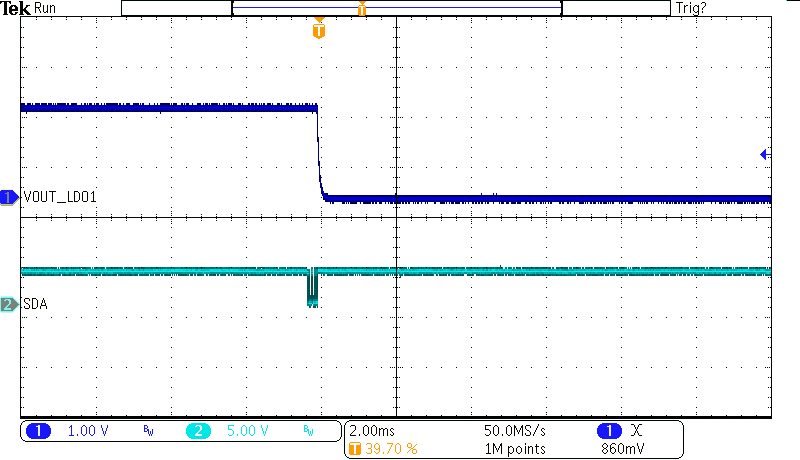
BQ25190 LDO1 Disable (No load)
VBAT = VSYS = VVINLS1 = 3.8V VLSLDO1 = 1.8V
Figure 8-25 LDO1 Disable (No load)
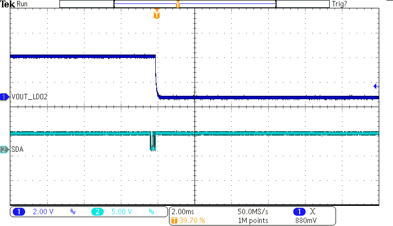
BQ25190 LDO2 Disable (No
                        load)
VBAT = VSYS = VVINLS2 = 3.8V VLSLDO2 = 3.3V
Figure 8-27 LDO2 Disable (No load)