SLUSBJ3F August 2013 – March 2019
PRODUCTION DATA.
- 1 Features
- 2 Applications
- 3 Description
- 4 Revision History
- 5 Pin Configuration and Functions
- 6 Specifications
- 7 Detailed Description
- 8 Application and Implementation
- 9 Power Supply Recommendations
- 10Layout
- 11Device and Documentation Support
- 12Mechanical, Packaging, and Orderable Information
Package Options
Mechanical Data (Package|Pins)
- RGR|20
Thermal pad, mechanical data (Package|Pins)
- RGR|20
Orderable Information
6.6 Typical Characteristics
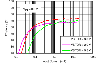
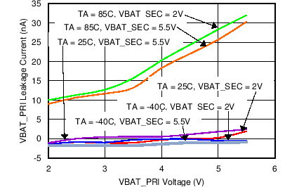
Unless otherwise noted, graphs were taken using Figure 28 with CIN = 4.7 µF, L1 = Coilcraft 22 µH LPS4018,CSTOR = 4.7 µF, VBAT_OV = 5 V
Table 1. Table of Graphs
| FIGURE | |||
|---|---|---|---|
| Charger Efficiency (η)(1) | vs. Input Voltage | IN= 10 µA | Figure 1 |
| IN= 100 µA | Figure 2 | ||
| IIN = 10 mA | Figure 3 | ||
| vs. Input Current | VIN = 2.0 V | Figure 4 | |
| VIN = 1.0 V | Figure 5 | ||
| VIN = 0.5 V | Figure 6 | ||
| VIN = 0.2 V | Figure 7 | ||
| VBAT_SEC Quiescent Current | vs. VBAT_SEC Voltage | EN = VBAT_SEC (Active Mode) | Figure 8 |
| EN = GND (Ship Mode) | Figure 9 | ||
| VBAT_PRI Leakage Current | vs. VBAT_PRI Voltage | EN = VBAT_SEC (Ship Mode) | Figure 10 |
(1) See SLUA691 for an explanation on how to take these measurements. Because the MPPT feature cannot be disabled on the bq25505, these measurements need to be taken in the middle of the 16 s sampling period.


| VIN_DC = Keithley Source Meter configured with ICOMP = 10 mA and voltage source varied from 0.1 V to 3.0 V |
| VSTOR = Keithley Sourcemeter configured to measure current and voltage source set to hold the VSTOR voltage = 2.0 V, 3.0 V or 5.5 V |

| VIN_DC = Keithley Source Meter configured with ICOMP = 100 µA and voltage source varied from 0.1 V to 3.0 V s | ||
| VSTOR = Keithley Sourcemeter configured to measure current and voltage source set to hold the VSTOR voltage = 2.0 V, 3.0 V or 5.5 V |

| VIN_DC = Keithley Source Meter configured with voltage source = 2.0 V and ICOMP varied from 0.01 mA to 100 mA |
| VSTOR = Keithley Sourcemeter configured to measure current and voltage source set to hold the VSTOR voltage = 2.2 V , 3.0 V or 5.5 V |

| VIN_DC = Keithley Source Meter configured with voltage source = 1.0 V and ICOMP varied from 0.01 mA to 100 mA |
| VSTOR = Keithley Sourcemeter configured to measure current and voltage source set to hold the VSTOR voltage = 2.0 V, 3.0 V or 5.5 V |

| VIN_DC = Keithley Source Meter configured with voltage source = 0.2 V and ICOMP varied from 0.01 mA to 100 mA |
| VSTOR = Keithley Sourcemeter configured to measure current and voltage source set to hold the VSTOR voltage = 2.0 V, 3.0 V or 5.5 V |

| VIN_DC = floating and EN = VBAT_SEC |
| VBAT_SEC = Keithley Sourcemeter configured to measure current and voltage source varied from 2.0 V or 5.5 V |
| VBAT_PRI = voltage source as indicated |

| VIN_DC = Keithley Source Meter configured with voltage source = 0.5 V and ICOMP varied from 0.01 mA to 100 mA |
| VSTOR = Keithley Sourcemeter configured to measure current and voltage source set to hold the VSTOR voltage = 1.8 V, 3.0 V or 5.5 V |

| VIN_DC = floating and EN = GND |
| VBAT_SEC = Keithley Sourcemeter configured to measure current and voltage source varied from 2.0 V or 5.5 V |
| VBAT_PRI = voltage source as indicated |

| VIN_DC = floating and EN = VBAT_SEC or GND |
| VBAT_PRI = Keithley Sourcemeter configured to measure current and voltage source varied from 2.0 V or 5.5 V |
| VBAT_SEC = voltage source as indicated |