SLUSEC9B October   2020  – July 2024 BQ25618E , BQ25619E

PRODUCTION DATA  

  1.   1
  2. Features
  3. Applications
  4. Description
  5. Description (continued)
  6. Device Comparison Table
  7. Pin Configuration and Functions
  8. Specifications
    1. 7.1 Absolute Maximum Ratings
    2. 7.2 ESD Ratings
    3. 7.3 Recommended Operating Conditions
    4. 7.4 Thermal Information
    5. 7.5 Electrical Characteristics
    6. 7.6 Timing Requirements
    7. 7.7 Typical Characteristics
  9. Detailed Description
    1. 8.1 Overview
    2. 8.2 Functional Block Diagram
    3. 8.3 Feature Description
      1. 8.3.1 Power-On-Reset (POR)
      2. 8.3.2 Device Power Up From Battery Without Input Source
      3. 8.3.3 Power Up From Input Source
        1. 8.3.3.1 Power Up REGN LDO
        2. 8.3.3.2 Poor Source Qualification
        3. 8.3.3.3 Input Source Type Detection (IINDPM Threshold)
          1. 8.3.3.3.1 PSEL Pins Sets Input Current Limit
        4. 8.3.3.4 Input Voltage Limit Threshold Setting (VINDPM Threshold)
        5. 8.3.3.5 Power Up Converter in Buck Mode
        6. 8.3.3.6 HIZ Mode with Adapter Present
      4. 8.3.4 Power Path Management
        1. 8.3.4.1 Narrow Voltage DC (NVDC) Architecture
        2. 8.3.4.2 Dynamic Power Management
        3. 8.3.4.3 Supplement Mode
      5. 8.3.5 Battery Charging Management
        1. 8.3.5.1 Autonomous Charging Cycle
        2. 8.3.5.2 Battery Charging Profile
        3. 8.3.5.3 Charging Termination
        4. 8.3.5.4 Thermistor Qualification
          1. 8.3.5.4.1 JEITA Guideline Compliance During Charging Mode
        5. 8.3.5.5 Charging Safety Timer
      6. 8.3.6 Ship Mode and QON Pin
        1. 8.3.6.1 BATFET Disable (Enter Ship Mode)
        2. 8.3.6.2 BATFET Enable (Exit Ship Mode)
        3. 8.3.6.3 BATFET Full System Reset
      7. 8.3.7 Status Outputs ( STAT, INT , PG )
        1. 8.3.7.1 Power Good Indicator (PG_STAT Bit; BQ25619E only)
        2. 8.3.7.2 Charging Status Indicator (STAT)
        3. 8.3.7.3 Interrupt to Host ( INT)
      8. 8.3.8 Protections
        1. 8.3.8.1 Voltage and Current Monitoring in Buck Mode
          1. 8.3.8.1.1 Input Overvoltage Protection (ACOV)
          2. 8.3.8.1.2 System Overvoltage Protection (SYSOVP)
        2. 8.3.8.2 Thermal Regulation and Thermal Shutdown
          1. 8.3.8.2.1 Thermal Protection in Buck Mode
        3. 8.3.8.3 Battery Protection
          1. 8.3.8.3.1 Battery Overvoltage Protection (BATOVP)
          2. 8.3.8.3.2 Battery Overdischarge Protection
          3. 8.3.8.3.3 System Overcurrent Protection
      9. 8.3.9 Serial Interface
        1. 8.3.9.1 Data Validity
        2. 8.3.9.2 START and STOP Conditions
        3. 8.3.9.3 Byte Format
        4. 8.3.9.4 Acknowledge (ACK) and Not Acknowledge (NACK)
        5. 8.3.9.5 Slave Address and Data Direction Bit
        6. 8.3.9.6 Single Read and Write
        7. 8.3.9.7 Multi-Read and Multi-Write
    4. 8.4 Device Functional Modes
      1. 8.4.1 Host Mode and Default Mode
    5. 8.5 Register Maps
  10. Application and Implementation
    1. 9.1 Application Information
    2. 9.2 Typical Application
      1. 9.2.1 Design Requirements
      2. 9.2.2 Detailed Design Procedure
        1. 9.2.2.1 Inductor Selection
        2. 9.2.2.2 Input Capacitor and Resistor
        3. 9.2.2.3 Output Capacitor
      3. 9.2.3 Application Curves
  11. 10Power Supply Recommendations
  12. 11Layout
    1. 11.1 Layout Guidelines
    2. 11.2 Layout Example
  13. 12Device and Documentation Support
    1. 12.1 Device Support
      1. 12.1.1 Third-Party Products Disclaimer
    2. 12.2 Documentation Support
      1. 12.2.1 Related Documentation
    3. 12.3 Receiving Notification of Documentation Updates
    4. 12.4 Support Resources
    5. 12.5 Trademarks
    6. 12.6 Electrostatic Discharge Caution
    7. 12.7 Glossary
  14. 13Revision History
  15. 14Mechanical, Packaging, and Orderable Information

Package Options

Refer to the PDF data sheet for device specific package drawings

Mechanical Data (Package|Pins)
  • RTW|24
Thermal pad, mechanical data (Package|Pins)
Orderable Information

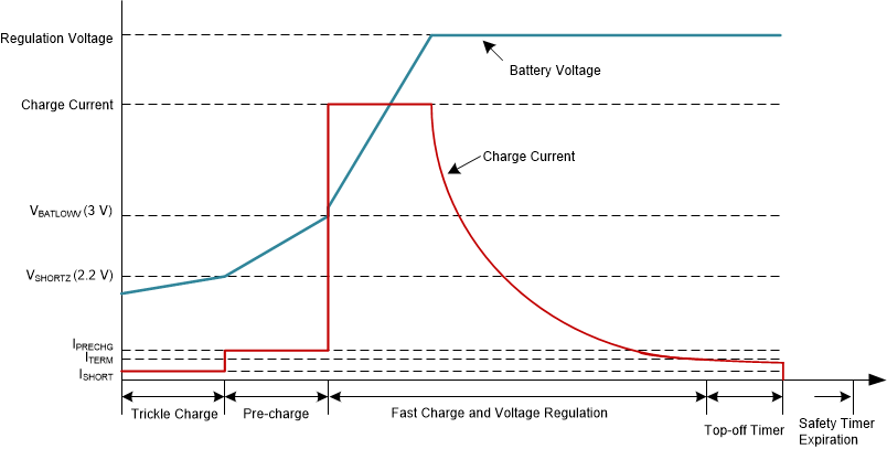
Battery Charging Profile

The device charges the battery in five phases: battery short, preconditioning, constant current, constant voltage and top-off trickle charging (optional). At the beginning of a charging cycle, the device checks the battery voltage and regulates current and voltage accordingly.

Resistance between charger output and battery cell terminal such as board routing, connector, MOSFETs and sense resistor can force the charging process to move from constant current to constant voltage too early and increase charge time. To speed up the charging cycle, the device provides BATSNS pin to extend the constant current charge time to deliver maximum power to battery. BATSNS pin should be connected directly to battery cell terminal to remotely sense battery cell voltage. When battery voltage is above VBAT_DPLZ, charger will detect whether the BATSNS pin is connected to BAT or not.

  • If BATSNS pin is not connected to BAT, BATSNS_DIS = 1, and charger regulates battery voltage through the BAT pin
  • If BATSNS pin is connected to BAT, BATFET_DIS = 0, and charger regulates battery voltage through the BATSNS pin

When battery voltage is below VBAT_DPLZ, charger will automatically regulate charge voltage through BAT pin without BATSNS detection.

  • When battery voltage rises above VBAT_DPLZ, host can set BATSNS_DIS to 0, to initiate BATSNS detection
Table 8-3 Charging Current Setting
VBAT CHARGING CURRENT DEFAULT SETTING CHRG_STAT
< 2.2 V IBAT_SHORT 25 mA 01
2.2 V to 3 V IPRECHG 40 mA 01
> 3 V ICHG 340 mA 10
BQ25618E BQ25619E Battery
                    Charging Profile Figure 8-2 Battery Charging Profile