SLUSEC9B October   2020  – July 2024 BQ25618E , BQ25619E

PRODUCTION DATA  

  1.   1
  2. Features
  3. Applications
  4. Description
  5. Description (continued)
  6. Device Comparison Table
  7. Pin Configuration and Functions
  8. Specifications
    1. 7.1 Absolute Maximum Ratings
    2. 7.2 ESD Ratings
    3. 7.3 Recommended Operating Conditions
    4. 7.4 Thermal Information
    5. 7.5 Electrical Characteristics
    6. 7.6 Timing Requirements
    7. 7.7 Typical Characteristics
  9. Detailed Description
    1. 8.1 Overview
    2. 8.2 Functional Block Diagram
    3. 8.3 Feature Description
      1. 8.3.1 Power-On-Reset (POR)
      2. 8.3.2 Device Power Up From Battery Without Input Source
      3. 8.3.3 Power Up From Input Source
        1. 8.3.3.1 Power Up REGN LDO
        2. 8.3.3.2 Poor Source Qualification
        3. 8.3.3.3 Input Source Type Detection (IINDPM Threshold)
          1. 8.3.3.3.1 PSEL Pins Sets Input Current Limit
        4. 8.3.3.4 Input Voltage Limit Threshold Setting (VINDPM Threshold)
        5. 8.3.3.5 Power Up Converter in Buck Mode
        6. 8.3.3.6 HIZ Mode with Adapter Present
      4. 8.3.4 Power Path Management
        1. 8.3.4.1 Narrow Voltage DC (NVDC) Architecture
        2. 8.3.4.2 Dynamic Power Management
        3. 8.3.4.3 Supplement Mode
      5. 8.3.5 Battery Charging Management
        1. 8.3.5.1 Autonomous Charging Cycle
        2. 8.3.5.2 Battery Charging Profile
        3. 8.3.5.3 Charging Termination
        4. 8.3.5.4 Thermistor Qualification
          1. 8.3.5.4.1 JEITA Guideline Compliance During Charging Mode
        5. 8.3.5.5 Charging Safety Timer
      6. 8.3.6 Ship Mode and QON Pin
        1. 8.3.6.1 BATFET Disable (Enter Ship Mode)
        2. 8.3.6.2 BATFET Enable (Exit Ship Mode)
        3. 8.3.6.3 BATFET Full System Reset
      7. 8.3.7 Status Outputs ( STAT, INT , PG )
        1. 8.3.7.1 Power Good Indicator (PG_STAT Bit; BQ25619E only)
        2. 8.3.7.2 Charging Status Indicator (STAT)
        3. 8.3.7.3 Interrupt to Host ( INT)
      8. 8.3.8 Protections
        1. 8.3.8.1 Voltage and Current Monitoring in Buck Mode
          1. 8.3.8.1.1 Input Overvoltage Protection (ACOV)
          2. 8.3.8.1.2 System Overvoltage Protection (SYSOVP)
        2. 8.3.8.2 Thermal Regulation and Thermal Shutdown
          1. 8.3.8.2.1 Thermal Protection in Buck Mode
        3. 8.3.8.3 Battery Protection
          1. 8.3.8.3.1 Battery Overvoltage Protection (BATOVP)
          2. 8.3.8.3.2 Battery Overdischarge Protection
          3. 8.3.8.3.3 System Overcurrent Protection
      9. 8.3.9 Serial Interface
        1. 8.3.9.1 Data Validity
        2. 8.3.9.2 START and STOP Conditions
        3. 8.3.9.3 Byte Format
        4. 8.3.9.4 Acknowledge (ACK) and Not Acknowledge (NACK)
        5. 8.3.9.5 Slave Address and Data Direction Bit
        6. 8.3.9.6 Single Read and Write
        7. 8.3.9.7 Multi-Read and Multi-Write
    4. 8.4 Device Functional Modes
      1. 8.4.1 Host Mode and Default Mode
    5. 8.5 Register Maps
  10. Application and Implementation
    1. 9.1 Application Information
    2. 9.2 Typical Application
      1. 9.2.1 Design Requirements
      2. 9.2.2 Detailed Design Procedure
        1. 9.2.2.1 Inductor Selection
        2. 9.2.2.2 Input Capacitor and Resistor
        3. 9.2.2.3 Output Capacitor
      3. 9.2.3 Application Curves
  11. 10Power Supply Recommendations
  12. 11Layout
    1. 11.1 Layout Guidelines
    2. 11.2 Layout Example
  13. 12Device and Documentation Support
    1. 12.1 Device Support
      1. 12.1.1 Third-Party Products Disclaimer
    2. 12.2 Documentation Support
      1. 12.2.1 Related Documentation
    3. 12.3 Receiving Notification of Documentation Updates
    4. 12.4 Support Resources
    5. 12.5 Trademarks
    6. 12.6 Electrostatic Discharge Caution
    7. 12.7 Glossary
  14. 13Revision History
  15. 14Mechanical, Packaging, and Orderable Information

Package Options

Refer to the PDF data sheet for device specific package drawings

Mechanical Data (Package|Pins)
  • RTW|24
Thermal pad, mechanical data (Package|Pins)
Orderable Information

BATFET Full System Reset

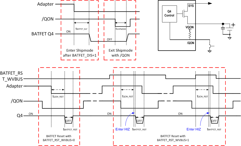
The BATFET functions as a load switch between battery and system when input source is not plugged in. When BATFET_RST_EN = 1 and BATFET_DIS = 0, BATFET full system reset function is enabled. By changing the state of BATFET from on to off, systems connected to SYS can be effectively forced to have a power-on-reset. After the reset is complete, device is in POR state, and all the registers are in POR default settings. The QON pin supports push-button interface to reset system power without host by changing the state of BATFET. Internally, it is pulled up to the VQON voltage through a 200-kΩ resistor.

When the QON pin is driven to logic low for tQON_RST, BATFET reset process starts. The BATFET is turned off for tBATFET_RST and then it is re-enabled to reset system power. This function can be disabled by setting BATFET_RST_EN bit to 0.

BATFET full system reset functions either with or without adapter present. If BATFET_RST_WVBUS = 1, the system reset function starts after tQON_RST when QON pin is pushed to LOW. Once the reset process starts, the device first goes into HIZ mode to turn off the converter, and then power cycles BATFET. If BATFET_RST_WVBUS = 0, the system reset function does not start until tQON_RST after QON pin is pushed to LOW and adapter is removed.

After BATFET full system reset is complete, the device will power up again if EN_HIZ is not set to 1 before the system reset.
BQ25618E BQ25619E QON TimingFigure 8-5 QON Timing