SLUSCQ8A May   2017  – May 2018

PRODUCTION DATA.  

  1. Features
  2. Applications
  3. Description
    1.     Device Images
      1.      Application Diagram
  4. Revision History
  5. Description (continued)
  6. Pin Configuration and Functions
    1.     Pin Functions
  7. Specifications
    1. 7.1 Absolute Maximum Ratings
    2. 7.2 ESD Ratings
    3. 7.3 Recommended Operating Conditions
    4. 7.4 Thermal Information
    5. 7.5 Electrical Characteristics
    6. 7.6 Timing Requirements
    7. 7.7 Typical Characteristics
  8. Detailed Description
    1. 8.1 Overview
    2. 8.2 Functional Block Diagram
    3. 8.3 Feature Description
      1. 8.3.1 Power-Up from Battery Without DC Source
      2. 8.3.2 Power-Up From DC Source
        1. 8.3.2.1 CHRG_OK Indicator
        2. 8.3.2.2 Input Voltage and Current Limit Setup
        3. 8.3.2.3 Battery Cell Configuration
        4. 8.3.2.4 Device Hi-Z State
      3. 8.3.3 USB On-The-Go (OTG)
      4. 8.3.4 Converter Operation
        1. 8.3.4.1 Inductor Setting through IADPT Pin
        2. 8.3.4.2 Continuous Conduction Mode (CCM)
        3. 8.3.4.3 Pulse Frequency Modulation (PFM)
      5. 8.3.5 Current and Power Monitor
        1. 8.3.5.1 High-Accuracy Current Sense Amplifier (IADPT and IBAT)
        2. 8.3.5.2 High-Accuracy Power Sense Amplifier (PSYS)
      6. 8.3.6 Input Source Dynamic Power Manage
      7. 8.3.7 Two-Level Adapter Current Limit (Peak Power Mode)
      8. 8.3.8 Processor Hot Indication
        1. 8.3.8.1 PROCHOT During Low Power Mode
        2. 8.3.8.2 PROCHOT Status
      9. 8.3.9 Device Protection
        1. 8.3.9.1 Watchdog Timer
        2. 8.3.9.2 Input Overvoltage Protection (ACOV)
        3. 8.3.9.3 Input Overcurrent Protection (ACOC)
        4. 8.3.9.4 System Overvoltage Protection (SYSOVP)
        5. 8.3.9.5 Battery Overvoltage Protection (BATOVP)
        6. 8.3.9.6 Battery Short
        7. 8.3.9.7 Thermal Shutdown (TSHUT)
    4. 8.4 Device Functional Modes
      1. 8.4.1 Forward Mode
        1. 8.4.1.1 System Voltage Regulation with Narrow VDC Architecture
        2. 8.4.1.2 Battery Charging
      2. 8.4.2 USB On-The-Go
    5. 8.5 Programming
      1. 8.5.1 SMBus Interface
        1. 8.5.1.1 SMBus Write-Word and Read-Word Protocols
        2. 8.5.1.2 Timing Diagrams
    6. 8.6 Register Map
      1. 8.6.1  Setting Charge and PROCHOT Options
        1. 8.6.1.1 ChargeOption0 Register (SMBus address = 12h) [reset = E20Eh]
          1. Table 7. ChargeOption0 Register (SMBus address = 12h) Field Descriptions
          2. Table 8. ChargeOption0 Register (SMBus address = 12h) Field Descriptions
        2. 8.6.1.2 ChargeOption1 Register (SMBus address = 30h) [reset = 211h]
          1. Table 9.   ChargeOption1 Register (SMBus address = 30h) Field Descriptions
          2. Table 10. ChargeOption1 Register (SMBus address = 30h) Field Descriptions
        3. 8.6.1.3 ChargeOption2 Register (SMBus address = 31h) [reset = 2B7]
          1. Table 11. ChargeOption2 Register (SMBus address = 31h) Field Descriptions
          2. Table 12. ChargeOption2 Register (SMBus address = 31h) Field Descriptions
        4. 8.6.1.4 ChargeOption3 Register (SMBus address = 32h) [reset = 0h]
          1. Table 13. ChargeOption3 Register (SMBus address = 32h) Field Descriptions
          2. Table 14. ChargeOption3 Register (SMBus address = 32h) Field Descriptions
        5. 8.6.1.5 ProchotOption0 Register (SMBus address = 33h) [reset = 04A54h]
          1. Table 15. ProchotOption0 Register (SMBus address = 33h) Field Descriptions
          2. Table 16. ProchotOption0 Register (SMBus address = 33h) Field Descriptions
        6. 8.6.1.6 ProchotOption1 Register (SMBus address = 34h) [reset = 8120h]
          1. Table 17. ProchotOption1 Register (SMBus address = 34h) Field Descriptions
          2. Table 18. ProchotOption1 Register (SMBus address = 34h) Field Descriptions
        7. 8.6.1.7 ADCOption Register (SMBus address = 35h) [reset = 2000h]
          1. Table 19. ADCOption Register (SMBus address = 35h) Field Descriptions
          2. Table 20. ADCOption Register (SMBus address = 35h) Field Descriptions
      2. 8.6.2  Charge and PROCHOT Status
        1. 8.6.2.1 ChargerStatus Register (SMBus address = 20h) [reset = 0000h]
          1. Table 21. ChargerStatus Register (SMBus address = 20h) Field Descriptions
          2. Table 22. ChargerStatus Register (SMBus address = 20h) Field Descriptions
        2. 8.6.2.2 ProchotStatus Register (SMBus address = 21h) [reset = 0h]
          1. Table 23. ProchotStatus Register (SMBus address = 21h) Field Descriptions
          2. Table 24. ProchotStatus Register (SMBus address = 21h) Field Descriptions
      3. 8.6.3  ChargeCurrent Register (SMBus address = 14h) [reset = 0h]
        1. Table 25. Charge Current Register (14h) With 10-mΩ Sense Resistor (SMBus address = 14h) Field Descriptions
        2. Table 26. Charge Current Register (14h) With 10-mΩ Sense Resistor (SMBus address = 14h) Field Descriptions
        3. 8.6.3.1    Battery Pre-Charge Current Clamp
      4. 8.6.4  MaxChargeVoltage Register (SMBus address = 15h) [reset value based on CELL_BATPRESZ pin setting]
        1. Table 27. MaxChargeVoltage Register (SMBus address = 15h) Field Descriptions
        2. Table 28. MaxChargeVoltage Register (SMBus address = 15h) Field Descriptions
      5. 8.6.5  MinSystemVoltage Register (SMBus address = 3Eh) [reset value based on CELL_BATPRESZ pin setting]
        1. Table 29. MinSystemVoltage Register (SMBus address = 3Eh) Field Descriptions
        2. Table 30. MinSystemVoltage Register (SMBus address = 3Eh) Field Descriptions
        3. 8.6.5.1    System Voltage Regulation
      6. 8.6.6  Input Current and Input Voltage Registers for Dynamic Power Management
        1. 8.6.6.1 Input Current Registers
          1. 8.6.6.1.1 IIN_HOST Register With 10-mΩ Sense Resistor (SMBus address = 3Fh) [reset = 4000h]
            1. Table 31. IIN_HOST Register With 10-mΩ Sense Resistor (SMBus address = 3Fh) Field Descriptions
            2. Table 32. IIN_HOST Register With 10-mΩ Sense Resistor (SMBus address = 3Fh) Field Descriptions
          2. 8.6.6.1.2 IIN_DPM Register With 10-mΩ Sense Resistor (SMBus address = 022h) [reset = 0h]
            1. Table 33. IIN_DPM Register With 10-mΩ Sense Resistor (SMBus address = 022h) Field Descriptions
            2. Table 34. IIN_DPM Register With 10-mΩ Sense Resistor (SMBus address = 022h) Field Descriptions
          3. 8.6.6.1.3 InputVoltage Register (SMBus address = 3Dh) [reset = VBUS-1.28V]
            1. Table 35. InputVoltage Register (SMBus address = 3Dh) Field Descriptions
            2. Table 36. InputVoltage Register (SMBus address = 3Dh) Field Descriptions
      7. 8.6.7  OTGVoltage Register (SMBus address = 3Bh) [reset = 0h]
        1. Table 37. OTGVoltage Register (SMBus address = 3Bh) Field Descriptions
        2. Table 38. OTGVoltage Register (SMBus address = 3Bh) Field Descriptions
      8. 8.6.8  OTGCurrent Register (SMBus address = 3Ch) [reset = 0h]
        1. Table 39. OTGCurrent Register (SMBus address = 3Ch) Field Descriptions
        2. Table 40. OTGCurrent Register (SMBus address = 3Ch) Field Descriptions
      9. 8.6.9  ADCVBUS/PSYS Register (SMBus address = 23h)
        1. Table 41. ADCVBUS/PSYS Register Field Descriptions
      10. 8.6.10 ADCIBAT Register (SMBus address = 24h)
        1. Table 42. ADCIBAT Register Field Descriptions
      11. 8.6.11 ADCIINCMPIN Register (SMBus address = 25h)
        1. Table 43. ADCIINCMPIN Register Field Descriptions
      12. 8.6.12 ADCVSYSVBAT Register (SMBus address = 26h)
        1. Table 44. ADCVSYSVBAT Register Field Descriptions
      13. 8.6.13 ID Registers
        1. 8.6.13.1 ManufactureID Register (SMBus address = FEh) [reset = 0040h]
          1. Table 45. ManufactureID Register Field Descriptions
        2. 8.6.13.2 Device ID (DeviceAddress) Register (SMBus address = FFh) [reset = 0h]
          1. Table 46. Device ID (DeviceAddress) Register Field Descriptions
  9. Application and Implementation
    1. 9.1 Application Information
    2. 9.2 Typical Application
      1. 9.2.1 Design Requirements
      2. 9.2.2 Detailed Design Procedure
        1. 9.2.2.1 ACP-ACN Input Filter
        2. 9.2.2.2 Inductor Selection
        3. 9.2.2.3 Input Capacitor
        4. 9.2.2.4 Output Capacitor
        5. 9.2.2.5 Power MOSFETs Selection
      3. 9.2.3 Application Curves
  10. 10Power Supply Recommendations
  11. 11Layout
    1. 11.1 Layout Guidelines
    2. 11.2 Layout Example
      1. 11.2.1 Layout Consideration of Current Path
      2. 11.2.2 Layout Consideration of Short Circuit Protection
  12. 12Device and Documentation Support
    1. 12.1 Device Support
      1. 12.1.1 Third-Party Products Disclaimer
    2. 12.2 Documentation Support
      1. 12.2.1 Related Documentation
    3. 12.3 Receiving Notification of Documentation Updates
    4. 12.4 Community Resources
    5. 12.5 Trademarks
    6. 12.6 Electrostatic Discharge Caution
    7. 12.7 Glossary
  13. 13Mechanical, Packaging, and Orderable Information

Package Options

Mechanical Data (Package|Pins)
Thermal pad, mechanical data (Package|Pins)
Orderable Information

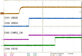
Application Curves

bq25700A W1_Powerup_20V_sluscp0.gif
2-cell without battery
Figure 42. Power Up from 20 V
bq25700A W3_Poweroff_12V_sluscp0.gif
3-cell VBAT = 10 V
Figure 44. Power Off from 12 V
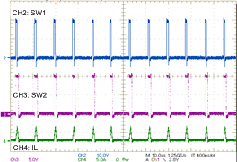
bq25700A W5_PFM_op_sluscp0.gif
VBUS = 20 V, VSYS = 10 V, ISYS = 200 mA
Figure 46. PFM Operation
bq25700A W7_Switch_During_Boost_sluscp0.gif
VBUS = 5 V, VBAT = 10 V
Figure 48. Switching During Boost Mode
bq25700A W9_Sys_Reg_Buck_sluscp0.gif
VBUS = 12 V/3.3 A, 3-cell, VSYS = 9 V, Without battery
Figure 50. System Regulation in Buck Mode
bq25700A W11_Sys_Reg_Boost_sluscp0.gif
VBUS = 5 V/3.3 A, 3-cell, VSYS = 9 V, Without battery
Figure 52. System Regulation in Boost Mode
bq25700A W13_IIN_Reg_Boost_sluscp0.gif
VBUS = 5 V/3.3 V, VBAT = 7.5 V
Figure 54. Input Current in Boost Mode
bq25700A W15_OTG_VOL_Rampup_sluscp0.gif
VBAT = 10 V, VBUS 5 V to 20 V, IOTG = 500 mA
Figure 56. OTG Voltage Ramp Up
bq25700A W17_OTG_Load_Trans_sluscp0.gif
VBAT = 10 V, VBUS = 20 V
Figure 58. OTG Load Transient
bq25700A W2_Powerup_5V_sluscp0.gif
2-cell without battery
Figure 43. Power Up from 5 V
bq25700A W4_SysReg_sluscp0.gif
VBUS 5 V to 20 V
Figure 45. System Regulation
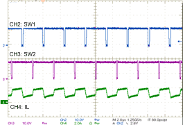
bq25700A W6_PWM_Op_sluscp0.gif
Figure 47. PWM Operation
bq25700A W8_Switch_Buck_Boost_sluscp0.gif
VBUS = 12 V, VBAT = 12 V
Figure 49. Switching During Buck Boost Mode
bq25700A W10_Sys_Reg_Buck_Boost_sluscp0.gif
VBUS = 9 V/3.3 A, 3-cell, VSYS = 9 V, Without battery
Figure 51. System Regulation in Buck Boost Mode
bq25700A W12_IIN_Reg_Buck_sluscp0.gif
VBUS = 20 V/3.3 V, VBAT = 7.5 V
Figure 53. Input Current Regulation in Buck Mode
bq25700A W14_OTG_Pwrup_8VBat_sluscp0.gif
VBUS = 5 V
Figure 55. OTG Power Up from 8 V Battery
bq25700A W16_OTG_Pwr_Off_sluscp0.gif
Figure 57. OTG Power Off