SLUSD20B july 2018 – april 2023 BQ25710
PRODUCTION DATA
- 1 Features
- 2 Applications
- 3 Description
- 4 Revision History
- 5 Description (continued)
- 6 Device Comparison Table
- 7 Pin Configuration and Functions
- 8 Specifications
-
9 Detailed Description
- 9.1 Overview
- 9.2 Functional Block Diagram
- 9.3
Feature Description
- 9.3.1 Power-Up from Battery Without DC Source
- 9.3.2 Vmin Active Protection (VAP) when Battery only Mode
- 9.3.3 Power-Up From DC Source
- 9.3.4 USB On-The-Go (OTG)
- 9.3.5 Converter Operation
- 9.3.6 Current and Power Monitor
- 9.3.7 Input Source Dynamic Power Manage
- 9.3.8 Two-Level Adapter Current Limit (Peak Power Mode)
- 9.3.9 Processor Hot Indication
- 9.3.10
Device Protection
- 9.3.10.1 Watchdog Timer
- 9.3.10.2 Input Overvoltage Protection (ACOV)
- 9.3.10.3 Input Overcurrent Protection (ACOC)
- 9.3.10.4 System Overvoltage Protection (SYSOVP)
- 9.3.10.5 Battery Overvoltage Protection (BATOVP)
- 9.3.10.6 Battery Short
- 9.3.10.7 System Short Hiccup Mode
- 9.3.10.8 Thermal Shutdown (TSHUT)
- 9.4 Device Functional Modes
- 9.5 Programming
- 9.6
Register Map
- 9.6.1
Setting Charge and
PROCHOT Options
- 9.6.1.1 ChargeOption0 Register (SMBus address = 12h) [reset = E70Eh]
- 9.6.1.2 ChargeOption1 Register (SMBus address = 30h) [reset = 0211h]
- 9.6.1.3 ChargeOption2 Register (SMBus address = 31h) [reset = 02B7h]
- 9.6.1.4 ChargeOption3 Register (SMBus address = 32h) [reset = 0030h]
- 9.6.1.5 ProchotOption0 Register (SMBus address = 33h) [reset = 4A65h]
- 9.6.1.6 ProchotOption1 Register (SMBus address = 34h) [reset = 81A0h]
- 9.6.1.7 ADCOption Register (SMBus address = 35h) [reset = 2000h]
- 9.6.2 Charge and PROCHOT Status
- 9.6.3 ChargeCurrent Register (SMBus address = 14h) [reset = 0000h]
- 9.6.4 MaxChargeVoltage Register (SMBus address = 15h) [reset value based on CELL_BATPRESZ pin setting]
- 9.6.5 MinSystemVoltage Register (SMBus address = 3Eh) [reset value based on CELL_BATPRESZ pin setting]
- 9.6.6 Input Current and Input Voltage Registers for Dynamic Power Management
- 9.6.7 OTGVoltage Register (SMBus address = 3Bh) [reset = 0000h]
- 9.6.8 OTGCurrent Register (SMBus address = 3Ch) [reset = 0000h]
- 9.6.9 ADCVBUS/PSYS Register (SMBus address = 23h)
- 9.6.10 ADCIBAT Register (SMBus address = 24h)
- 9.6.11 ADCIINCMPIN Register (SMBus address = 25h)
- 9.6.12 ADCVSYSVBAT Register (SMBus address = 26h)
- 9.6.13 ID Registers
- 9.6.1
Setting Charge and
PROCHOT Options
- 10Application and Implementation
- 11Power Supply Recommendations
- 12Layout
- 13Device and Documentation Support
- 14Mechanical, Packaging, and Orderable Information
Package Options
Mechanical Data (Package|Pins)
- RSN|32
Thermal pad, mechanical data (Package|Pins)
- RSN|32
Orderable Information
9.3.9 Processor Hot Indication
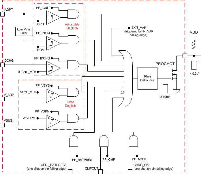
When CPU is running turbo mode, the system peak power may exceed available power from adapter and battery together. The adapter current and battery discharge peak current, or system voltage drop is an indication that system power is too high. The charger processor hot function monitors these events, and PROCHOT pulse is asserted if the system power is too high. Once CPU receives PROCHOT pulse from charger, it slows down to reduce system power. The events monitored by the processor hot function includes:
- ICRIT: adapter peak current, as 110% of ILIM2
- INOM: adapter average current (110% of input current limit)
- IDCHG: battery discharge current
- VSYS: system voltage on VSYS
- Adapter Removal: upon adapter removal (CHRG_OK pin HIGH to LOW)
- Battery Removal: upon battery removal (CELL_BATPRESZ pin goes LOW)
- CMPOUT: Independent comparator output (CMPOUT pin HIGH to LOW)
- VDPM: VBUS lower than 80%/90%/100% of VINDPM threshold.
- EXIT_VAP: Every time when the charger exits VAP mode.
The threshold of ICRIT, IDCHG, VSYS or VDPM, and the deglitch time of ICRIT, INOM, IDCHG or CMPOUT are programmable through SMBus. Except the PROCHOT_EXIT_VAP is always enabled, the other triggering events can be individually enabled in REG0x34[7:0]. When any enabled event in PROCHOT profile is triggered, PROCHOT is asserted low for a single pulse with minimal width programmable in REG0x21[13:12]. At the end of the single pulse, if the PROCHOT event is still active, the pulse gets extended until the event is removed.
If the PROCHOT pulse extension mode is enabled by setting REG0x21[14] = 1, the PROCHOT pin will be kept as low until host writes REG0x21[11]21[11] = 0, even if the triggering event has been removed.
If the PROCHOT_VDPM or PROCHOT_EXIT_VAP is triggered, PROCHOT pin will always stay low until the host clears it, no matter the PROCHOT is in one pulse mod or in extended mode.
 Figure 9-2 PROCHOT Profile