SLUSD83C june 2018 – may 2023 BQ25713 , BQ25713B
PRODUCTION DATA
- 1
- 1 Features
- 2 Applications
- 3 Description
- 4 Revision History
- 5 Description (continued)
- 6 Device Comparison Table
- 7 Pin Configuration and Functions
- 8 Specifications
-
9 Detailed Description
- 9.1 Overview
- 9.2 Functional Block Diagram
- 9.3
Feature Description
- 9.3.1 Power-Up from Battery Without DC Source
- 9.3.2 Vmin Active Protection (VAP) when Battery only Mode
- 9.3.3 Power-Up From DC Source
- 9.3.4 USB On-The-Go (OTG)
- 9.3.5 Converter Operation
- 9.3.6 Current and Power Monitor
- 9.3.7 Input Source Dynamic Power Manage
- 9.3.8 Two-Level Adapter Current Limit (Peak Power Mode)
- 9.3.9 Processor Hot Indication
- 9.3.10
Device Protection
- 9.3.10.1 Watchdog Timer
- 9.3.10.2 Input Overvoltage Protection (ACOV)
- 9.3.10.3 Input Overcurrent Protection (ACOC)
- 9.3.10.4 System Overvoltage Protection (SYSOVP)
- 9.3.10.5 Battery Overvoltage Protection (BATOVP)
- 9.3.10.6 Battery Short
- 9.3.10.7 System Short Hiccup Mode
- 9.3.10.8 Thermal Shutdown (TSHUT)
- 9.4 Device Functional Modes
- 9.5 Programming
- 9.6
Register Map
- 9.6.1
Setting Charge and
PROCHOT Options
- 9.6.1.1 ChargeOption0 Register (I2C address = 01/00h) [reset = E70Eh]
- 9.6.1.2 ChargeOption1 Register (I2C address = 31/30h) [reset = 0211h]
- 9.6.1.3 ChargeOption2 Register (I2C address = 33/32h) [reset = 02B7h]
- 9.6.1.4 ChargeOption3 Register (I2C address = 35/34h) [reset = 0030h]
- 9.6.1.5 ProchotOption0 Register (I2C address = 37/36h) [reset = 4A65h]
- 9.6.1.6 ProchotOption1 Register (I2C address = 39/38h) [reset = 81A0h]
- 9.6.1.7 ADCOption Register (I2C address = 3B/3Ah) [reset = 2000h]
- 9.6.2 Charge and PROCHOT Status
- 9.6.3 ChargeCurrent Register (I2C address = 03/02h) [reset = 0000h]
- 9.6.4 MaxChargeVoltage Register (I2C address = 05/04h) [reset value based on CELL_BATPRESZ pin setting]
- 9.6.5 MinSystemVoltage Register (I2C address = 0D/0Ch) [reset value based on CELL_BATPRESZ pin setting]
- 9.6.6 Input Current and Input Voltage Registers for Dynamic Power Management
- 9.6.7 OTGVoltage Register (I2C address = 07/06h) [reset = 0000h]
- 9.6.8 OTGCurrent Register (I2C address = 09/08h) [reset = 0000h]
- 9.6.9 ADCVBUS/PSYS Register (I2C address = 27/26h)
- 9.6.10 ADCIBAT Register (I2C address = 29/28h)
- 9.6.11 ADCIINCMPIN Register (I2C address = 2B/2Ah)
- 9.6.12 ADCVSYSVBAT Register (I2C address = 2D/2Ch)
- 9.6.13 ID Registers
- 9.6.1
Setting Charge and
PROCHOT Options
- 10Application and Implementation
- 11Power Supply Recommendations
- 12Layout
- 13Device and Documentation Support
- 14Mechanical, Packaging, and Orderable Information
Package Options
Mechanical Data (Package|Pins)
- RSN|32
Thermal pad, mechanical data (Package|Pins)
- RSN|32
Orderable Information
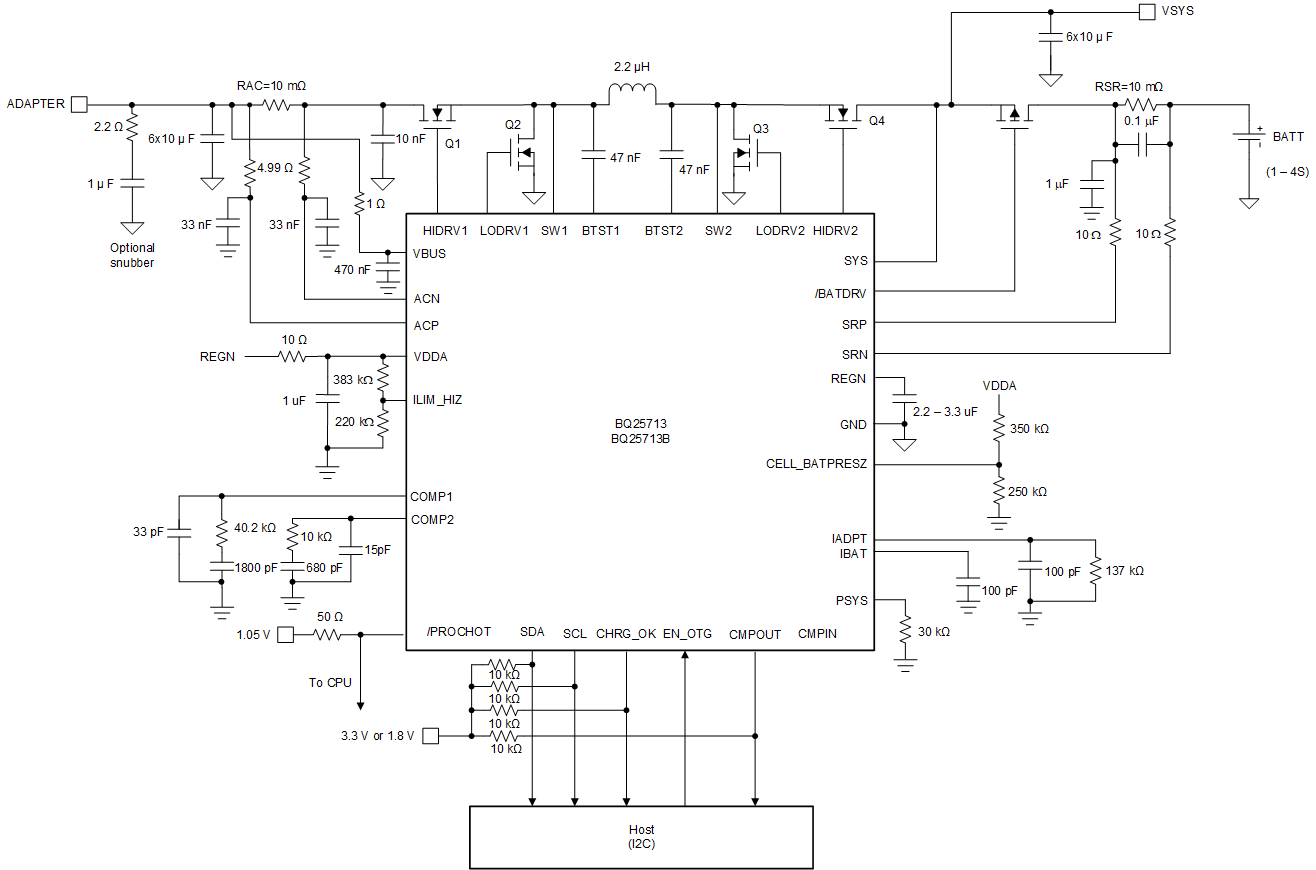
10.2 Typical Application
 Figure 10-1 Application
Diagram