SLUSEK7 September 2024 BQ25773
PRODUCTION DATA
- 1
- 1 Features
- 2 Applications
- 3 Description
- 4 Device Comparison Table
- 5 Pin Configuration and Functions
- 6 Specifications
-
7 Detailed Description
- 7.1 Overview
- 7.2 Functional Block Diagram
- 7.3
Feature Description
- 7.3.1 Power-Up Sequence
- 7.3.2 MODE Pin Detection
- 7.3.3 REGN Regulator (REGN LDO)
- 7.3.4 Independent Comparator Function
- 7.3.5 Battery Charging Management
- 7.3.6 Temperature Regulation (TREG)
- 7.3.7 Vmin Active Protection (VAP) When Battery Only Mode
- 7.3.8 Two Level Battery Discharge Current Limit
- 7.3.9 Fast Role Swap Feature
- 7.3.10 CHRG_OK Indicator
- 7.3.11 Input and Charge Current Sensing
- 7.3.12 Input Current and Voltage Limit Setup
- 7.3.13 Battery Cell Configuration
- 7.3.14 Device HIZ State
- 7.3.15 USB On-The-Go (OTG)
- 7.3.16 Quasi Dual Phase Converter Operation
- 7.3.17 Continuous Conduction Mode (CCM)
- 7.3.18 Pulse Frequency Modulation (PFM)
- 7.3.19 Switching Frequency and Dithering Feature
- 7.3.20 Current and Power Monitor
- 7.3.21 Input Source Dynamic Power Management
- 7.3.22 Integrated 16-Bit ADC for Monitoring
- 7.3.23 Input Current Optimizer (ICO)
- 7.3.24 Two-Level Adapter Current Limit (Peak Power Mode)
- 7.3.25 Processor Hot Indication
- 7.3.26
Device Protection
- 7.3.26.1 Watchdog Timer (WD)
- 7.3.26.2 Input Overvoltage Protection (ACOV)
- 7.3.26.3 Input Overcurrent Protection (ACOC)
- 7.3.26.4 System Overvoltage Protection (SYSOVP)
- 7.3.26.5 Battery Overvoltage Protection (BATOVP)
- 7.3.26.6 Battery Charge Overcurrent Protection (BATCOC)
- 7.3.26.7 Battery Discharge Overcurrent Protection (BATDOC)
- 7.3.26.8 BATFET Charge Current Clamp Protection under LDO Regulation Mode
- 7.3.26.9 Sleep Comparator Protection Between VBUS and ACP_A (SC_VBUSACP)
- 7.3.26.10 High Duty Buck Exit Comparator Protection (HDBCP)
- 7.3.26.11 REGN Power Good Protection (REGN_PG)
- 7.3.26.12 System Under Voltage Lockout (VSYS_UVP) and Hiccup Mode
- 7.3.26.13 OTG Mode Over Voltage Protection (OTG_OVP)
- 7.3.26.14 OTG Mode Under Voltage Protection (OTG_UVP)
- 7.3.26.15 Thermal Shutdown (TSHUT)
- 7.4 Device Functional Modes
- 7.5 Programming
- 7.6 BQ25773 Registers
- 8 Application and Implementation
- 9 Power Supply Recommendations
- 10Layout
- 11Device and Documentation Support
- 12Revision History
- 13Mechanical, Packaging, and Orderable Information
Package Options
Refer to the PDF data sheet for device specific package drawings
Mechanical Data (Package|Pins)
- REE|36
Thermal pad, mechanical data (Package|Pins)
Orderable Information
8.2.2.4 Input Capacitor
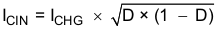
Input capacitor should have enough ripple current rating to absorb input switching ripple current. The worst case RMS ripple current is half of the charging current (plus system current there is any system load) when duty cycle is 0.5 in buck mode. If the converter does not operate at 50% duty cycle, then the worst case capacitor RMS current occurs where the duty cycle is closest to 50% and can be estimated by Equation 5:
Low ESR ceramic capacitor such as X7R or X5R is preferred for input decoupling capacitor and should be placed in front of RAC current sensing and as close as possible to the power stage half bridge MOSFETs. Capacitance after RAC before power stage half bridge should be limited to10μF+10nF+1nF referring to Figure 8-3 diagram. Voltage rating of the capacitor must be higher than normal input voltage level, 35 V rating or higher capacitor is preferred for 28 V input voltage. Minimum 10 pieces of 10-µF 0603 size capacitors are suggested for 28V/140 W adapter design. 50-V rating or higher capacitor is preferred for 36-V input voltage. Minimum 10*10μF 0805 capacitors are needed when power reaches 36 V/180 W. Under different input voltage the minimum input capacitance requirement is summarized in Table 8-7, Table 8-3 and Table 8-4. For quasi dual phase it is recommended to spread the MLCC caps before RAC_A and RAC_B. 1*10nF+1nF 0402 package MLCC capacitors (EMI filter purpose) are recommended to be placed as close as possible to both phase A and phase B half bridge MOSFETs.
Ceramic capacitors show a dc-bias effect. This effect reduces the effective capacitance when a dc-bias voltage is applied across a ceramic capacitor, as on the input capacitor of a charger. The effect may lead to a significant capacitance drop, especially for high input voltages and small capacitor packages. See the manufacturer's data sheet about the derating performance with a dc bias voltage applied. It may be necessary to choose a higher voltage rating or nominal capacitance value in order to get the required capacitance value at the operating point. Tantalum capacitors (POSCAP) can avoid dc-bias effect and temperature variation effect which is recommended especially for 28-V and 36-V higher power application.
| 20-V/100-W SYSTEM | MINIMUM | TYPICAL | MAXIMUM |
|---|---|---|---|
| Effective input capacitance |
4 μF (MLCC) OTG is not needed 8 μF (MLCC) OTG is needed |
4 μF (MLCC) + 15 μF (POSCAP) | 4 μF (MLCC) + 2*33 μF (POSCAP) |
| Practical input capacitors configuration |
4*10 μF OTG is not needed (0603 35 V MLCC derating to around 10% under 20-V bias voltage) |
4*10 μF (0603 35 V MLCC derating to around 10% under 20-V bias voltage) 1*15 μF (2917 35 V POSCAP) |
4*10 μF (0603 35 V MLCC derating to around 10% under 20-V bias voltage) 2*33 μF (2917 35 V POSCAP) |
| 28-V/140-W SYSTEM | MINIMUM | TYPICAL | MAXIMUM |
|---|---|---|---|
| Effective input capacitance |
6 μF (MLCC) OTG is not needed 8 μF (MLCC) OTG is needed |
6 μF (MLCC) + 15 μF (POSCAP) | 6 μF (MLCC) + 2*33 μF (POSCAP) |
| Practical input capacitors configuration |
10*10 μF OTG is not needed (0603 35 V MLCC derating to around 6% under 28-V bias voltage) |
10*10 μF (0603 35 V MLCC derating to around 6% under 28-V bias voltage ) 1*15 μF (2917 35 V POSCAP) |
10*10 μF (0603 35 V MLCC derating to around 6% under 28-V bias voltage ) 2*33 μF (2917 35 V POSCAP) |
| 36-V/180-W SYSTEM | MINIMUM | TYPICAL | MAXIMUM |
|---|---|---|---|
| Effective input capacitance | 8 μF (MLCC) | 8 μF (MLCC) + 15 μF (POSCAP) | 8 μF (MLCC) + 2*33 μF (POSCAP) |
| Practical input capacitors configuration |
10*10 μF (0805 50 V MLCC derating to around 8% under 36-V bias voltage) |
10*10 μF (0805 50 V MLCC derating to around 8% under 36-V bias voltage) 1*15 μF (2917 50 V POSCAP) |
10*10 μF (0805 50 V MLCC derating to around 8% under 36-V bias voltage) 2*33 μF (2917 50 V POSCAP) |