SLUSEK7 September 2024 BQ25773
PRODUCTION DATA
- 1
- 1 Features
- 2 Applications
- 3 Description
- 4 Device Comparison Table
- 5 Pin Configuration and Functions
- 6 Specifications
-
7 Detailed Description
- 7.1 Overview
- 7.2 Functional Block Diagram
- 7.3
Feature Description
- 7.3.1 Power-Up Sequence
- 7.3.2 MODE Pin Detection
- 7.3.3 REGN Regulator (REGN LDO)
- 7.3.4 Independent Comparator Function
- 7.3.5 Battery Charging Management
- 7.3.6 Temperature Regulation (TREG)
- 7.3.7 Vmin Active Protection (VAP) When Battery Only Mode
- 7.3.8 Two Level Battery Discharge Current Limit
- 7.3.9 Fast Role Swap Feature
- 7.3.10 CHRG_OK Indicator
- 7.3.11 Input and Charge Current Sensing
- 7.3.12 Input Current and Voltage Limit Setup
- 7.3.13 Battery Cell Configuration
- 7.3.14 Device HIZ State
- 7.3.15 USB On-The-Go (OTG)
- 7.3.16 Quasi Dual Phase Converter Operation
- 7.3.17 Continuous Conduction Mode (CCM)
- 7.3.18 Pulse Frequency Modulation (PFM)
- 7.3.19 Switching Frequency and Dithering Feature
- 7.3.20 Current and Power Monitor
- 7.3.21 Input Source Dynamic Power Management
- 7.3.22 Integrated 16-Bit ADC for Monitoring
- 7.3.23 Input Current Optimizer (ICO)
- 7.3.24 Two-Level Adapter Current Limit (Peak Power Mode)
- 7.3.25 Processor Hot Indication
- 7.3.26
Device Protection
- 7.3.26.1 Watchdog Timer (WD)
- 7.3.26.2 Input Overvoltage Protection (ACOV)
- 7.3.26.3 Input Overcurrent Protection (ACOC)
- 7.3.26.4 System Overvoltage Protection (SYSOVP)
- 7.3.26.5 Battery Overvoltage Protection (BATOVP)
- 7.3.26.6 Battery Charge Overcurrent Protection (BATCOC)
- 7.3.26.7 Battery Discharge Overcurrent Protection (BATDOC)
- 7.3.26.8 BATFET Charge Current Clamp Protection under LDO Regulation Mode
- 7.3.26.9 Sleep Comparator Protection Between VBUS and ACP_A (SC_VBUSACP)
- 7.3.26.10 High Duty Buck Exit Comparator Protection (HDBCP)
- 7.3.26.11 REGN Power Good Protection (REGN_PG)
- 7.3.26.12 System Under Voltage Lockout (VSYS_UVP) and Hiccup Mode
- 7.3.26.13 OTG Mode Over Voltage Protection (OTG_OVP)
- 7.3.26.14 OTG Mode Under Voltage Protection (OTG_UVP)
- 7.3.26.15 Thermal Shutdown (TSHUT)
- 7.4 Device Functional Modes
- 7.5 Programming
- 7.6 BQ25773 Registers
- 8 Application and Implementation
- 9 Power Supply Recommendations
- 10Layout
- 11Device and Documentation Support
- 12Revision History
- 13Mechanical, Packaging, and Orderable Information
Package Options
Refer to the PDF data sheet for device specific package drawings
Mechanical Data (Package|Pins)
- REE|36
Thermal pad, mechanical data (Package|Pins)
Orderable Information
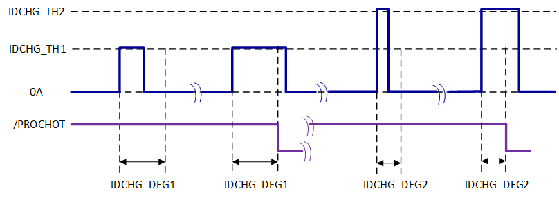
7.3.8 Two Level Battery Discharge Current Limit
To prevent the triggering of battery overcurrent protection and avoid battery wear-out, two battery current limit levels (IDCHG_TH1 and IDCHG_TH2) PROCHOT profiles are recommended. Define IDCHG_TH1 through REG0x39/38h[7:2], IDCHG_TH2 is set through REG0x3D/3Ch[5:3] for fixed percentage of IDCHG_TH1. There are dedicated deglitch time setting registers (IDCHG_DEG1 and IDCHG_DEG2) for both IDCHG_TH1 and IDCHG_TH2.
- When battery discharge
current is continuously higher than IDCHG_TH1 for more than IDCHG_DEG1
deglitch time, PROCHOT is asserted immediately. If the
discharge current reduces to lower than IDCHG_TH1, then the IDCHG_DEG1
deglitch time counter resets automatically. STAT_IDCHG1 bit will be set to 1
after PROCHOT is triggered.
Setting PP_IDCHG1=1b to enable IDCHG_TH1 for triggering PROCHOT.
- When battery discharge
current is continuously higher than IDCHG_TH2 for more than IDCHG_DEG2
deglitch time, PROCHOT is asserted immediately. If the
discharge current reduces to lower than IDCHG_TH2, then the IDCHG_DEG2
deglitch time counter resets automatically. STAT_IDCHG2 bit will be set to 1
after PROCHOT is triggered.
Setting PP_IDCHG2=1b to enable IDCHG_TH2 for triggering PROCHOT.
 Figure 7-8 Two Level Battery Discharging
Current Trigger PROCHOT Diagram