SLUSD88A March 2019 – June 2019 BQ25886
PRODUCTION DATA.
- 1 Features
- 2 Applications
- 3 Description
- 4 Revision History
- 5 Device Comparison Table
- 6 Pin Configuration and Functions
- 7 Specifications
-
8 Detailed Description
- 8.1 Overview
- 8.2 Functional Block Diagram
- 8.3
Feature Description
- 8.3.1 Device Power-On-Reset
- 8.3.2 Device Power Up from Battery without Input Source
- 8.3.3 Device Power Up from Input Source
- 8.3.4 Input Current Optimizer (ICO)
- 8.3.5 Buck Mode Operation from Battery (OTG)
- 8.3.6 PowerPath Management
- 8.3.7 Battery Charging Management
- 8.3.8 Status Outputs
- 8.3.9 Input Current Limit on ILIM Pin
- 8.3.10 Voltage and Current Monitoring
- 8.3.11 Thermal Regulation and Thermal Shutdown
- 8.3.12 Battery Protection
- 8.4 Device Functional Modes
- 9 Application and Implementation
- 10Power Supply Recommendations
- 11Layout
- 12Device and Documentation Support
- 13Mechanical, Packaging, and Orderable Information
Package Options
Mechanical Data (Package|Pins)
- RGE|24
Thermal pad, mechanical data (Package|Pins)
- RGE|24
Orderable Information
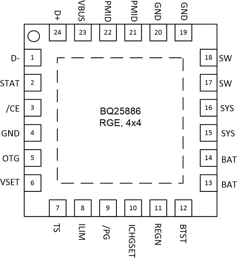
6 Pin Configuration and Functions
RGE Package (Standalone)
24-Pin VQFN
Top View

Pin Functions
| PIN | I/O | DESCRIPTION | |
|---|---|---|---|
| NAME | NO. | ||
| D+ | 24 | AIO | Positive USB data line – D+/D– based USB host/charging port detection. The detection includes data contact detection (DCD) and secondary detection in BC1.2. |
| D– | 1 | AIO | Negative USB data line – D+/D– based USB host/charging port detection. The detection includes data contact detection (DCD) and secondary detection in BC1.2. |
| STAT | 2 | DO | Open drain charge status indicator – Connect to the pull-up rail via 10-kΩ resistor. LOW indicates charge in progress. HIGH indicates charge complete or charge disabled. When any fault occurs, the STAT pin blinks at 1Hz. |
| CE | 3 | DI | Active Low Charge Enable Pin – Battery charging is enabled when CE pin is LOW. CE pin is internally pulled low with 900k-Ω resistor. |
| OTG | 5 | DI | OTG – USB On-The-Go Enable input. Pull high to enable OTG function. Pull low to disable OTG function. |
| VSET | 6 | AI | Battery Charge Voltage Limit – VSET pin sets battery charge voltage. Program battery regulation voltage with a resistor pull-down from VSET to GND as follows:
RVSET< 18kΩ (short to GND) = 8.2 V RVSET= 39kΩ (±10%) = 8.8 V RVSET= 75kΩ (±10%) = 8.7 V RVSET> 150kΩ (floating) = 8.4 V |
| TS | 7 | AI | Temperature Qualification Voltage – Connect a negative temperature coefficient thermistor. Program temperature window with a resistor divider from REGN to TS to GND. Charge suspends when TS pin is out of range. Recommend 103AT-2 thermistor. |
| ILIM | 8 | AI | Input Current Limit (IINDPM) – ILIM pin sets the maximum input current and can be used to monitor input current. IINDPM loop regulates ILIM pin voltage at 0.8V. When ILIM pin is less than 0.8V, the input current can be calculated by IIN = KILIM x VILIM / (RILIM x 0.8V). A resistor connected from ILIM pin to ground sets the input current limit as maximum (IINMAX = KILIM / RILIM). When ILIM pin is short to GND, the input current limit is set to maximum by ILIM. Input current limit less than 500mA is not supported on ILIM pin. Do not float this pin.
|
| PG | 9 | DO | Open drain active low power good indicator – Connect to the pull up rail via 10-kΩ resistor. LOW indicates a good input source if the input voltage is within VVBUS_OP (3.9 V), and can provide more than IPOORSRC (30 mA). |
| ICHGSET | 10 | AI | Charge Current Limit – A resistor from ICHGSET to GND is used to program the charge current. The acceptable programming range on ICHGSET pin is 30mA (114Ω) – 2.2A (8kΩ). Pre-charge and termination current is 1/10 of the fast charge current. The minimum pre-charge current is clamped at 30mA (typ). Minimum termination current is clamped at 10mA (typ). ICHGSET short to GND clamps charge current to minimum setting 30mA (typ). Floating ICHGSET disables charge. |
| REGN | 11 | P | Gate Drive Supply – Bias supply for internal MOSFETs driver and IC. Bypass REGN to GND with a 4.7-µF ceramic capacitor. REGN current limit is 50 mA. |
| BTST | 12 | P | PWM High-side Driver Supply – Internally, BTST is connected to the cathode of the boot-strap diode. Connect a 47nF bootstrap capacitor from SW to BTST. |
| BAT | 13, 14 | P | Battery Power Connection – Connect minimum recommended 10-µF capacitance after derating closely to the BAT pin and GND. |
| SYS | 15, 16 | P | System Connection – The internal BATFET is connected between SYS and BAT. When the battery falls below the minimum system voltage, the switch-mode converter keeps SYS above the minimum system voltage. Connect a 2x22-µF capacitance after derating closely to the SYS pin and PGND. |
| SW | 17, 18 | P | Inductor Connection – Connect to the switched side of the external inductor. |
| GND | 19, 20, 4 | – | Ground Return |
| PMID | 21, 22 | P | Blocking MOSFET Connection – The minimum recommended total input low-ESR capacitance on VBUS and PMID, after applied derating, is 10 uF. At least 1-uF is recommended at VBUS with the remainder at PMID. Typical value for PMID is 10 uF. |
| VBUS | 23 | P | Input Supply – VBUS is connected to the external DC supply. Bypass VBUS to GND with at least 1-µF ceramic capacitor, placed as close to the IC as possible. |
| NC | 1 | – | No Connect – Leave these pins floating or tie to ground. |