SLUSD89B February   2019  – November 2019 BQ25887

PRODUCTION DATA.  

  1. Features
  2. Applications
  3. Description
    1.     Simplified Schematic
  4. Revision History
  5. Device Comparison Table
  6. Pin Configuration and Functions
    1.     Pin Functions
  7. Specifications
    1. 7.1 Absolute Maximum Ratings
    2. 7.2 ESD Ratings
    3. 7.3 Recommended Operating Conditions
    4. 7.4 Thermal Information
    5. 7.5 Electrical Characteristics
    6. 7.6 Timing Requirements
    7. 7.7 Typical Characteristics
  8. Detailed Description
    1. 8.1 Overview
    2. 8.2 Functional Block Diagram
    3. 8.3 Feature Description
      1. 8.3.1  Device Power-On-Reset
      2. 8.3.2  Device Power Up from Input Source
        1. 8.3.2.1 Poor Source Qualification
        2. 8.3.2.2 Input Source Type Detection
          1. 8.3.2.2.1 PSEL Sets Input Current Limit
          2. 8.3.2.2.2 Force Input Current Limit Detection
        3. 8.3.2.3 Power Up REGN Regulator (LDO)
        4. 8.3.2.4 Converter Power Up
      3. 8.3.3  Input Current Optimizer (ICO)
      4. 8.3.4  Battery Charging Management
        1. 8.3.4.1 Autonomous Charging Cycle
        2. 8.3.4.2 Battery Charging Profile
        3. 8.3.4.3 Cell Balancing During Charging
        4. 8.3.4.4 Charging Termination
        5. 8.3.4.5 Thermistor Qualification
          1. 8.3.4.5.1 JEITA Guideline Compliance in Charge Mode
        6. 8.3.4.6 Charging Safety Timer
      5. 8.3.5  Integrated 16-Bit ADC for Monitoring
      6. 8.3.6  Status Outputs
        1. 8.3.6.1 Power Good Indicator (PG)
        2. 8.3.6.2 Charging Status Indicator (STAT)
        3. 8.3.6.3 Interrupt to Host
      7. 8.3.7  Input Current Limit on ILIM Pin
      8. 8.3.8  Voltage and Current Monitoring
        1. 8.3.8.1 Voltage and Current Monitoring in Boost Mode
          1. 8.3.8.1.1 Input Over-Voltage Protection
          2. 8.3.8.1.2 Input Under-Voltage Protection
      9. 8.3.9  Thermal Regulation and Thermal Shutdown
        1. 8.3.9.1 Thermal Protection in Boost Mode
      10. 8.3.10 Battery Protection
      11. 8.3.11 Serial Interface
        1. 8.3.11.1 Data Validity
        2. 8.3.11.2 START and STOP Conditions
        3. 8.3.11.3 Byte Format
        4. 8.3.11.4 Acknowledge (ACK) and Not Acknowledge (NACK)
        5. 8.3.11.5 Slave Address and Data Direction Bit
        6. 8.3.11.6 Single Write and Read
        7. 8.3.11.7 Multi-Write and Multi-Read
    4. 8.4 Device Functional Modes
      1. 8.4.1 Host Mode and Default Mode
    5. 8.5 Register Maps
      1. 8.5.1  Cell Voltage Regulation Limit Register (Address = 00h) [reset = A0h]
        1. Table 8. REG00 Register Field Descriptions
      2. 8.5.2  Charger Current Limit Register (Address = 01h) [reset = 5Eh]
        1. Table 9. REG01 Register Field Descriptions
      3. 8.5.3  Input Voltage Limit Register (Address = 02h) [reset = 84h]
        1. Table 10. REG02 Register Field Descriptions
      4. 8.5.4  Input Current Limit Register (Address = 03h) [reset = 39h ]
        1. Table 11. REG03 Register Field Descriptions
      5. 8.5.5  Precharge and Termination Current Limit Register (Address = 04h) [reset = 22h]
        1. Table 12. REG04 Register Field Descriptions
      6. 8.5.6  Charger Control 1 Register (Address = 05h) [reset = 9Dh]
        1. Table 13. REG05 Register Field Descriptions
      7. 8.5.7  Charger Control 2 Register (Address = 06h) [reset = 7Dh]
        1. Table 14. REG06 Register Field Descriptions
      8. 8.5.8  Charger Control 3 Register (Address = 07h) [reset = 00h]
        1. Table 15. REG07 Register Field Descriptions
      9. 8.5.9  Charger Control 4 Register (Address = 08h) [reset = 0Dh]
        1. Table 16. REG08 Register Field Descriptions
      10. 8.5.10 Reserved Register (Address = 09h) [reset = 00h]
        1. Table 17. REG09 Register Field Descriptions
      11. 8.5.11 ICO Current Limit in Use Register (Address = 0Ah) [reset = XXh]
        1. Table 18. REG0A Register Field Descriptions
      12. 8.5.12 Charger Status 1 Register (Address = 0Bh) [reset = XXh]
        1. Table 19. REG0B Register Field Descriptions
      13. 8.5.13 Charger Status 2 Register (Address = 0Ch) [reset = XXh]
        1. Table 20. REG0C Register Field Descriptions
      14. 8.5.14 NTC Status Register (Address = 0Dh) [reset = 0Xh]
        1. Table 21. REG0D Register Field Descriptions
      15. 8.5.15 FAULT Status Register (Address = 0Eh) [reset = XXh]
        1. Table 22. REG0E Register Field Descriptions
      16. 8.5.16 Charger Flag 1 Register (Address = 0Fh) [reset = 00h]
        1. Table 23. REG0F Register Field Descriptions
      17. 8.5.17 Charger Flag 2 Register (Address = 10h) [reset = 00h]
        1. Table 24. REG10 Register Field Descriptions
      18. 8.5.18 FAULT Flag Register (Address = 11h) [reset = 00h]
        1. Table 25. REG11 Register Field Descriptions
      19. 8.5.19 Charger Mask 1 Register (Address = 12h) [reset = 00h]
        1. Table 26. REG12 Register Field Descriptions
      20. 8.5.20 Charger Mask 2 Register (Address = 13h) [reset = 00h]
        1. Table 27. REG13 Register Field Descriptions
      21. 8.5.21 FAULT Mask Register (Address = 14h) [reset = 00h]
        1. Table 28. REG14 Register Field Descriptions
      22. 8.5.22 ADC Control Register (Address = 15h) [reset = 30h]
        1. Table 29. REG15 Register Field Descriptions
      23. 8.5.23 ADC Function Disable Register (Address = 16h) [reset = 00h]
        1. Table 30. REG16 Register Field Descriptions
      24. 8.5.24 IBUS ADC 1 Register (Address = 17h) [reset = 00h]
        1. Table 31. REG17 Register Field Descriptions
      25. 8.5.25 IBUS ADC 0 Register (Address = 18h) [reset = 00h]
        1. Table 32. REG18 Register Field Descriptions
      26. 8.5.26 ICHG ADC 1 Register (Address = 19h) [reset = 00h]
        1. Table 33. REG19 Register Field Descriptions
      27. 8.5.27 ICHG ADC 0 Register (Address = 1Ah) [reset = 00h]
        1. Table 34. REG1A Register Field Descriptions
      28. 8.5.28 VBUS ADC 1 Register (Address = 1Bh) [reset = 00h]
        1. Table 35. REG1B Register Field Descriptions
      29. 8.5.29 VBUS ADC 0 Register (Address = 1Ch) [reset = 00h]
        1. Table 36. REG1C Register Field Descriptions
      30. 8.5.30 VBAT ADC 1 Register (Address = 1Dh) [reset = 00h]
        1. Table 37. REG1D Register Field Descriptions
      31. 8.5.31 VBAT ADC 0 Register (Address = 1Eh) [reset = 00h]
        1. Table 38. REG1E Register Field Descriptions
      32. 8.5.32 VCELLTOP ADC 1 Register (Address = 1Fh) [reset = 00h]
        1. Table 39. REG1F Register Field Descriptions
      33. 8.5.33 VCELLTOP ADC 0 Register (Address = 20h) [reset = 00h]
        1. Table 40. REG20 Register Field Descriptions
      34. 8.5.34 TS ADC 1 Register (Address = 21h) [reset = 00h]
        1. Table 41. REG21 Register Field Descriptions
      35. 8.5.35 TS ADC 0 Register (Address = 22h) [reset = 00h]
        1. Table 42. REG22 Register Field Descriptions
      36. 8.5.36 TDIE ADC 1 Register (Address = 23h) [reset = 00h]
        1. Table 43. REG23 Register Field Descriptions
      37. 8.5.37 TDIE ADC 0 Register (Address = 24h) [reset = 00h]
        1. Table 44. REG24 Register Field Descriptions
      38. 8.5.38 Part Information Register (Address = 25h) [reset = 28h]
        1. Table 45. REG25 Register Field Descriptions
      39. 8.5.39 VCELLBOT ADC 1 Register (Address = 26h) [reset = 00h]
        1. Table 46. REG26 Register Field Descriptions
      40. 8.5.40 VCELLBOT ADC 0 Register (Address = 27h) [reset = 00h]
        1. Table 47. REG27 Register Field Descriptions
      41. 8.5.41 Cell Balancing Control 1 Register (Address = 28h) [reset = 2Ah]
        1. Table 48. REG28 Register Field Descriptions
      42. 8.5.42 Cell Balancing Control 2 Register (Address = 29h) [reset = F4h]
        1. Table 49. REG29 Register Field Descriptions
      43. 8.5.43 Cell Balancing Status and Control Register (Address = 2Ah) [reset = 81h]
        1. Table 50. REG2A Register Field Descriptions
      44. 8.5.44 Cell Balancing Flag Register (Address = 2Bh) [reset = 00h]
        1. Table 51. REG2B Register Field Descriptions
      45. 8.5.45 Cell Balancing Mask Register (Address = 2Ch) [reset = 00h]
        1. Table 52. REG2C Register Field Descriptions
  9. Application and Implementation
    1. 9.1 Application Information
    2. 9.2 Typical Application
      1. 9.2.1 Design Requirements
      2. 9.2.2 Detailed Design Procedure
        1. 9.2.2.1 Inductor Selection
        2. 9.2.2.2 Input (VBUS / PMID) Capacitor
        3. 9.2.2.3 Output (VSNS) Capacitor
      3. 9.2.3 Application Curves
  10. 10Power Supply Recommendations
  11. 11Layout
    1. 11.1 Layout Guidelines
    2. 11.2 Layout Example
  12. 12Device and Documentation Support
    1. 12.1 Device Support
      1. 12.1.1 Third-Party Products Disclaimer
    2. 12.2 Documentation Support
      1. 12.2.1 Related Documentation
    3. 12.3 Receiving Notification of Documentation Updates
    4. 12.4 Support Resources
    5. 12.5 Trademarks
    6. 12.6 Electrostatic Discharge Caution
    7. 12.7 Glossary
  13. 13Mechanical, Packaging, and Orderable Information

Package Options

Mechanical Data (Package|Pins)
Thermal pad, mechanical data (Package|Pins)
Orderable Information

Typical Characteristics

CVBUS = 1µF, CPMID= 10µF, CSNS= 44µF, CBAT = 10µF, L = 1µH (DFE252012F-1R0) (unless otherwise specified)
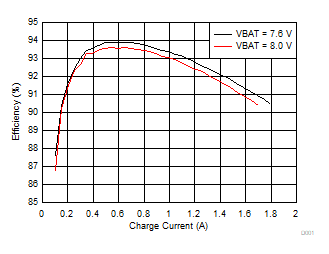
BQ25887 D001_SLUSD64_ChargeEfficiencyvsChargeCurrent.gif
VBUS = 5V
Figure 1. Charge Efficiency vs. Charge Current
BQ25887 D004_SLUSD64_ChargeCurrentAccuracyvsICHGSetting.gif
VBUS = 5V
Figure 3. Charge Current Accuracy vs. ICHG Setting
BQ25887 D012_SLUSD64_InputCurrenLimitAccuracyvsIINDPMSetting.gif
VBUS = 5.0V VBAT = 7.6V
Figure 5. Input Current Limit Accuracy vs. IINDPM Setting
BQ25887 D014_SLUSD64_TREG_Profiles.gif
VBUS = 5V VBAT = 7.6V ICHG = 100mA
Figure 7. TREG Profiles
BQ25887 D001_SLUSD64_L2inductor_ChargeEfficiencyvsChargeCurrent.gif
VBUS = 5V L = 1µH (IHLP2525CZER1R0k01)
Figure 2. Charge Efficiency vs. Charge Current
BQ25887 D004_SLUSD64_L2iinductor_ChargeCurrentAccuracyvsICHGSetting.gif
VBUS = 5V L = 1µH (IHLP2525CZER1R0k01)
Figure 4. Charge Current Accuracy vs. ICHG Setting
BQ25887 D013_SLUSD64_VINDPMSetting.gif
VBAT = 7.6V
Figure 6. Input Voltage Limit Accuracy vs. VINDPM Setting
BQ25887 D015_SLUSD64_MaxCurrentTemperatureProfile.gif
VBUS = 5V VBAT = 7.6V ICHG = 0.5A, 1.0A, 1.4A
Figure 8. Max Current Temperature Profile