SLUSB23B October 2012 – June 2015
PRODUCTION DATA.
- 1 Features
- 2 Applications
- 3 Description
- 4 Revision History
- 5 Device Comparison Table
- 6 Pin Configuration and Functions
-
7 Specifications
- 7.1 Absolute Maximum Ratings
- 7.2 ESD Ratings
- 7.3 Recommended Operating Conditions
- 7.4 Thermal Information
- 7.5 Electrical Characteristics: Power-On Reset
- 7.6 2.5-V LDO Regulator
- 7.7 Integrating ADC (Coulomb Counter) Characteristics
- 7.8 Integrated Sense Resistor Characteristics
- 7.9 ADC (Temperature and Cell Measurement) Characteristics
- 7.10 EEPROM Memory Characteristics
- 7.11 Timing Requirements: I2C-Compatible Interface Communication
- 7.12 Typical Characteristics
-
8 Detailed Description
- 8.1 Overview
- 8.2 Functional Block Diagram
- 8.3 Feature Description
- 8.4 Device Functional Modes
- 8.5
Programming
- 8.5.1
Standard Data Commands
- 8.5.1.1
Control(): 0x00 and 0x01
- 8.5.1.1.1 CONTROL_STATUS: 0x0000
- 8.5.1.1.2 DEVICE_TYPE: 0x0001
- 8.5.1.1.3 FW_VERSION: 0x0002
- 8.5.1.1.4 PREV_MACWRITE: 0x0007
- 8.5.1.1.5 CHEM_ID: 0x0008
- 8.5.1.1.6 BAT_INSERT: 0X000C
- 8.5.1.1.7 BAT_REMOVE: 0X000D
- 8.5.1.1.8 SET_HIBERNATE: 0x0011
- 8.5.1.1.9 CLEAR_HIBERNATE: 0x0012
- 8.5.1.1.10 SET_CFGUPDATE: 0x0013
- 8.5.1.1.11 SEALED: 0x0020
- 8.5.1.1.12 RESET: 0x0041
- 8.5.1.1.13 SOFT_RESET: 0x0042
- 8.5.1.2 Temperature( ): 0x02 and 0x03
- 8.5.1.3 Voltage( ): 0x04 and 0x05
- 8.5.1.4 Flags( ): 0x06 and 0x07
- 8.5.1.5 NominalAvailableCapacity( ): 0x08 and 0x09
- 8.5.1.6 FullAvailableCapacity( ): 0x0A and 0x0B
- 8.5.1.7 RemainingCapacity( ): 0x0C and 0x0D
- 8.5.1.8 FullChargeCapacity( ): 0x0E and 0x0F
- 8.5.1.9 AverageCurrent( ): 0x10 and 0x11
- 8.5.1.10 AveragePower( ): 0x18 and 0x19
- 8.5.1.11 StateOfCharge( ): 0x1C and 0x1D
- 8.5.1.12 IntTemperature( ): 0x1E and 0x1F
- 8.5.1.13 StateOfHealth( ): 0x20 and 0x21
- 8.5.1.14 OperationConfiguration( ): 0x3A and 0x3B
- 8.5.1.15 DesignCapacity( ): 0x3C and 0x3D
- 8.5.1.16 DebugX( ):
- 8.5.1.1
Control(): 0x00 and 0x01
- 8.5.2 Extended Data Commands
- 8.5.3 Block Data Interface
- 8.5.4 Access Modes
- 8.5.5 Data Block Summary
- 8.5.6 Detecting Charge Termination
- 8.5.7 Communications
- 8.5.1
Standard Data Commands
- 8.6 Register Maps
- 9 Application and Implementation
- 10Power Supply Recommendations
- 11Layout
- 12Device and Documentation Support
- 13Mechanical, Packaging, and Orderable Information
Package Options
Mechanical Data (Package|Pins)
- YZF|15
Thermal pad, mechanical data (Package|Pins)
Orderable Information
11 Layout
11.1 Layout Guidelines
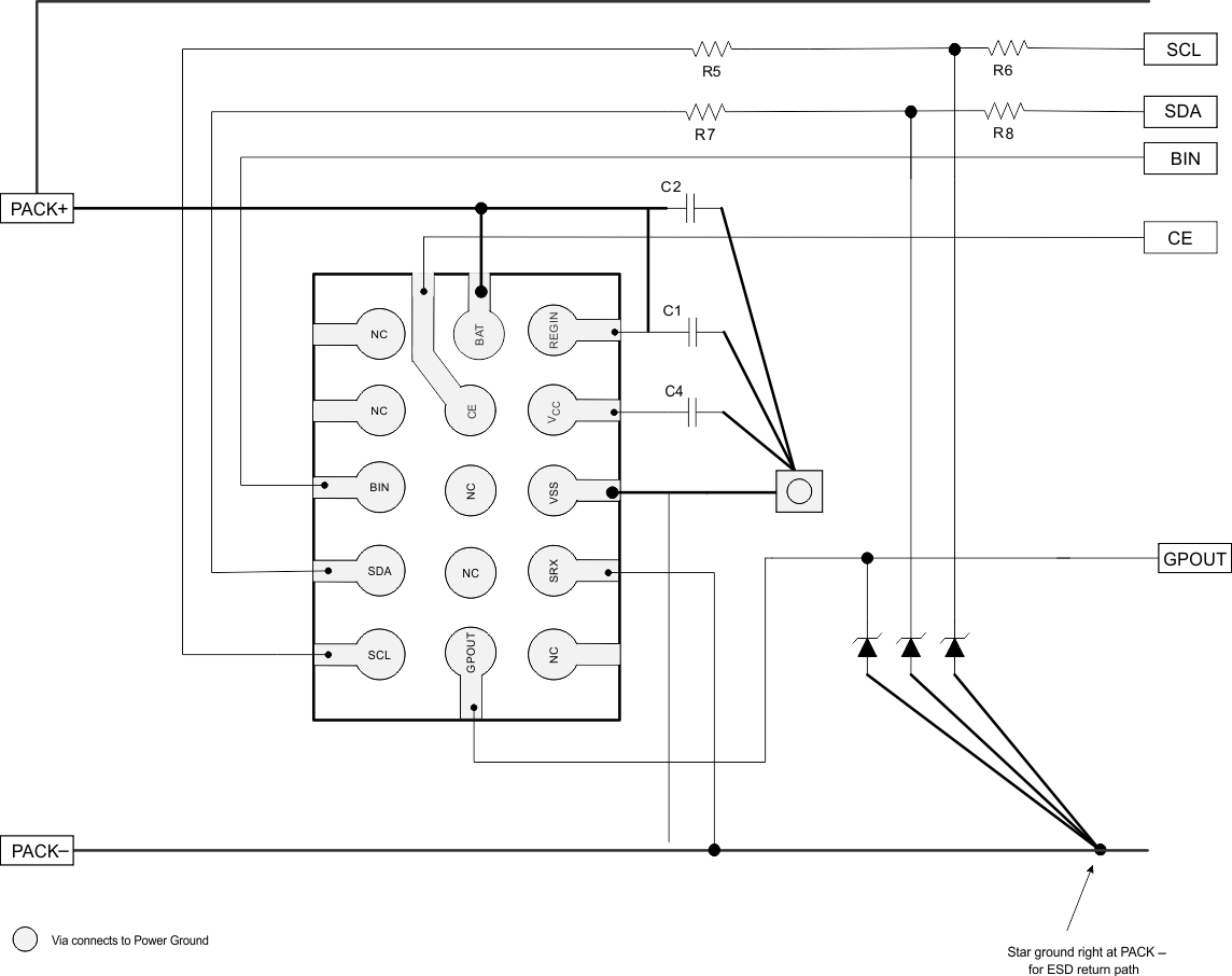
A capacitor of at least 1 μF is connected between the VCC pin and VSS. The capacitor should be placed close to the gauge IC and have short traces to both the VCC pin and VSS.
- A capacitor at least 0.1 μF must be connected between the BAT pin and VSS if the connection between the battery pack and the gauge BAT pin has the potential to pick up noise. The capacitor should be placed close to the gauge IC and have short traces to both the VDD pin and VSS.
- If the external pullup resistors on the SCL and SDA lines will be disconnected from the host during low-power operation, TI recommends using external 1-MΩ pulldown resistors to VSS to avoid floating inputs to the I2C engine.
- The value of the SCL and SDA pullup resistors should take into consideration the pullup voltage and the bus capacitance.
- If the GPOUT pin is not used by the host, the pin should still be pulled up to VDD with a 4.7-kΩ or 10-kΩ resistor.
- The BIN pin should not be shorted directly to VCC or VSS.
11.2 Layout Example
 Figure 16. Layout Schematic