SLUSAL5C December   2012  – June 2016

PRODUCTION DATA.  

  1. Features
  2. Applications
  3. Description
  4. Revision History
  5. Pin Configuration and Functions
  6. Specifications
    1. 6.1  Absolute Maximum Ratings
    2. 6.2  ESD Ratings
    3. 6.3  Thermal Information
    4. 6.4  Recommended Operating Conditions
    5. 6.5  Supply Current
    6. 6.6  Digital Input and Output DC Characteristics
    7. 6.7  Power-on Reset
    8. 6.8  2.5-V LDO Regulator
    9. 6.9  Internal Clock Oscillators
    10. 6.10 ADC (Temperature and Cell Measurement) Characteristics
    11. 6.11 Integrating ADC (Coulomb Counter) Characteristics
    12. 6.12 Data Flash Memory Characteristics
    13. 6.13 I2C-Compatible Interface Communication Timing Characteristics
    14. 6.14 Typical Characteristics
  7. Detailed Description
    1. 7.1 Overview
    2. 7.2 Functional Block Diagram
    3. 7.3 Feature Description
      1. 7.3.1 Functional Description
    4. 7.4 Device Functional Modes
      1. 7.4.1 Power Modes
        1. 7.4.1.1 BAT INSERT CHECK Mode
        2. 7.4.1.2 NORMAL Mode
        3. 7.4.1.3 SLEEP Mode
      2. 7.4.2 SLEEP+ Mode
      3. 7.4.3 HIBERNATE Mode
    5. 7.5 Programming
      1. 7.5.1 Standard Data Commands
      2. 7.5.2 Control(): 0x00/0x01
      3. 7.5.3 Communications
        1. 7.5.3.1 I2C Interface
        2. 7.5.3.2 I2C Time Out
        3. 7.5.3.3 I2C Command Waiting Time
        4. 7.5.3.4 I2C Clock Stretching
  8. Application and Implementation
    1. 8.1 Application Information
    2. 8.2 Typical Application
      1. 8.2.1 Design Requirements
      2. 8.2.2 Detailed Design Procedure
        1. 8.2.2.1 BAT Voltage Sense Input
        2. 8.2.2.2 SRP and SRN Current Sense Inputs
        3. 8.2.2.3 Sense Resistor Selection
        4. 8.2.2.4 TS Temperature Sense Input
        5. 8.2.2.5 Thermistor Selection
        6. 8.2.2.6 REGIN Power Supply Input Filtering
        7. 8.2.2.7 VCC LDO Output Filtering
      3. 8.2.3 Application Curves
  9. Power Supply Recommendations
    1. 9.1 Power Supply Decoupling
  10. 10Layout
    1. 10.1 Layout Guidelines
      1. 10.1.1 Sense Resistor Connections
      2. 10.1.2 Thermistor Connections
      3. 10.1.3 High-Current and Low-Current Path Separation
    2. 10.2 Layout Example
  11. 11Device and Documentation Support
    1. 11.1 Receiving Notification of Documentation Updates
    2. 11.2 Community Resource
    3. 11.3 Trademarks
    4. 11.4 Electrostatic Discharge Caution
    5. 11.5 Glossary
  12. 12Mechanical, Packaging, and Orderable Information

Package Options

Mechanical Data (Package|Pins)
Thermal pad, mechanical data (Package|Pins)
Orderable Information

8 Application and Implementation

NOTE

Information in the following applications sections is not part of the TI component specification, and TI does not warrant its accuracy or completeness. TI’s customers are responsible for determining suitability of components for their purposes. Customers should validate and test their design implementation to confirm system functionality.

8.1 Application Information

The fuel gauge can control a bq2416x Charger IC without the intervention from an application system processor. Using the bq27530-G1 and bq2416x chipset, batteries can be charged with the typical constant-current, constant-voltage (CCCV) profile or charged using a Multi-Level Charging (MLC) algorithm.

8.2 Typical Application

bq27530-G1 lusal5_TypApp.gif Figure 9. Typical Application

8.2.1 Design Requirements

Several key parameters must be updated to align with a given application's battery characteristics. For highest accuracy gauging, it is important to follow-up this initial configuration with a learning cycle to optimize resistance and maximum chemical capacity (Qmax) values prior to sealing and shipping systems to the field. Successful and accurate configuration of the fuel gauge for a target application can be used as the basis for creating a "golden" gas gauge (.fs) file that can be written to all gauges, assuming identical pack design and Li-ion cell origin (chemistry, lot, and so on). Calibration data is included as part of this golden GG file to cut down on system production time. If going this route, it is recommended to average the voltage and current measurement calibration data from a large sample size and use these in the golden file. Table 4, shows the items that should be configured to achieve reliable protection and accurate gauging with minimal initial configuration.

Table 4. Key Data Flash Parameters for Configuration

NAME DEFAULT UNIT RECOMMENDED SETTING
Design Capacity 1544 mAh Set based on the nominal pack capacity as interpreted from cell manufacturer's data sheet. If multiple parallel cells are used, should be set to N × Cell Capacity.
Reserve Capacity-mAh 0 mAh Set to desired runtime remaining (in seconds/3600) × typical applied load between reporting 0% SOC and reaching Terminate Voltage, if needed.
Cycle Count Threshold 1390 mAh Set to 90% of configured Design Capacity.
Chem ID 1189 hex Should be configured using TI-supplied Battery Management Studio software. Default open-circuit voltage and resistance tables are also updated in conjunction with this step. Do not attempt to manually update reported Device Chemistry as this does not change all chemistry information! Always update chemistry using the appropriate software tool (that is, bqStudio).
Load Mode 0 Set to applicable load model, 0 for constant current or 1 for constant power.
Load Select 1 Set to load profile which most closely matches typical system load.
Qmax Cell 0 1544 mAh Set to initial configured value for Design Capacity. The gauge will update this parameter automatically after the optimization cycle and for every regular Qmax update thereafter.
V at Chg Term Cell 0 4200 mV Set to nominal cell voltage for a fully charged cell. The gauge will update this parameter automatically each time full charge termination is detected.
Terminate Voltage 3200 mV Set to empty point reference of battery based on system needs. Typical is between 3000 mV and 3200 mV.
Ra Max Delta 44 Set to 15% of Cell0 R_a 4 resistance after an optimization cycle is completed.
Charging Voltage 4200 mV Set based on nominal charge voltage for the battery in normal conditions (25°C, etc). Used as the reference point for offsetting by Taper Voltage for full charge termination detection.
Taper Current 77 mA Set to the nominal taper current of the charger + taper current tolerance to ensure that the gauge will reliably detect charge termination.
Taper Voltage 100 mV Sets the voltage window for qualifying full charge termination. Can be set tighter to avoid or wider to ensure possibility of reporting 100% SOC in outer JEITA temperature ranges that use derated charging voltage.
Dsg Current Threshold 60 mA Sets threshold for gauge detecting battery discharge. Should be set lower than minimal system load expected in the application and higher than Quit Current.
Chg Current Threshold 75 mA Sets the threshold for detecting battery charge. Can be set higher or lower depending on typical trickle charge current used. Also should be set higher than Quit Current.
Quit Current 40 mA Sets threshold for gauge detecting battery relaxation. Can be set higher or lower depending on typical standby current and exhibited in the end system.
Avg I Last Run –299 mA Current profile used in capacity simulations at onset of discharge or at all times if Load Select = 0. Should be set to nominal system load. Is automatically updated by the gauge every cycle.
Avg P Last Run –1131 mW Power profile used in capacity simulations at onset of discharge or at all times if Load Select = 0. Should be set to nominal system power. Is automatically updated by the gauge every cycle.
Sleep Current 10 mA Sets the threshold at which the fuel gauge enters SLEEP mode. Take care in setting above typical standby currents else entry to SLEEP may be unintentionally blocked.
Charge T0 0 °C Sets the boundary between charging inhibit and charging with T0 parameters.
Charge T1 10 °C Sets the boundary between charging with T0 and T1 parameters.
Charge T2 45 °C Sets the boundary between charging with T1 and T2 parameters.
Charge T3 50 °C Sets the boundary between charging with T2 and T3 parameters.
Charge T4 60 °C Sets the boundary between charging with T3 and T4 parameters.
Charge Current T0 50 % Des Cap Sets the charge current parameter for T0.
Charge Current T1 100 % Des Cap Sets the charge current parameter for T1.
Charge Current T2 100 % Des Cap Sets the charge current parameter for T2.
Charge Current T3 100 % Des Cap Sets the charge current parameter for T3.
Charge Current T4 0 % Des Cap Sets the charge current parameter for T4.
Charge Voltage T0 210 20 mV Sets the charge voltage parameter for T0.
Charge Voltage T1 210 20 mV Sets the charge voltage parameter for T1.
Charge Voltage T2 207 20 mV Sets the charge voltage parameter for T2.
Charge Voltage T3 205 20 mV Sets the charge voltage parameter for T3.
Charge Voltage T4 0 20 mV Sets the charge voltage parameter for T4.
Chg Temp Hys 3 °C Adds temperature hysteresis for boundary crossings to avoid oscillation if temperature is changing by a degree or so on a given boundary.
Chg Disabled Regulation V 4200 mV Sets the voltage threshold for voltage regulation to system when charge is disabled. It is recommended to program to same value as Charging Voltage and maximum charge voltage that is obtained from Charge Voltage Tn parameters.
CC Gain 10 Calibrate this parameter using TI-supplied bqStudio software and calibration procedure in the TRM. Determines conversion of coulomb counter measured sense resistor voltage to current.
CC Delta 10 Calibrate this parameter using TI-supplied bqStudio software and calibration procedure in the TRM. Determines conversion of coulomb counter measured sense resistor voltage to passed charge.
CC Offset –1418 Counts Calibrate this parameter using TI-supplied bqStudio software and calibration procedure in the TRM. Determines native offset of coulomb counter hardware that should be removed from conversions.
Board Offset 0 Counts Calibrate this parameter using TI-supplied bqStudio software and calibration procedure in the TRM. Determines native offset of the printed circuit board parasitics that should be removed from conversions.
Pack V Offset 0 mV Calibrate this parameter using TI-supplied bqStudio software and calibration procedure in the TRM. Determines voltage offset between cell tab and ADC input node to incorporate back into or remove from measurement, depending on polarity.

8.2.2 Detailed Design Procedure

8.2.2.1 BAT Voltage Sense Input

A ceramic capacitor at the input to the BAT pin is used to bypass AC voltage ripple to ground, greatly reducing its influence on battery voltage measurements. It proves most effective in applications with load profiles that exhibit high-frequency current pulses (that is, cell phones) but is recommended for use in all applications to reduce noise on this sensitive high-impedance measurement node.

8.2.2.2 SRP and SRN Current Sense Inputs

The filter network at the input to the coulomb counter is intended to improve differential mode rejection of voltage measured across the sense resistor. These components should be placed as close as possible to the coulomb counter inputs and the routing of the differential traces length-matched to best minimize impedance mismatch-induced measurement errors.

8.2.2.3 Sense Resistor Selection

Any variation encountered in the resistance present between the SRP and SRN pins of the fuel gauge will affect the resulting differential voltage, and derived current, it senses. As such, it is recommended to select a sense resistor with minimal tolerance and temperature coefficient of resistance (TCR) characteristics. The standard recommendation based on best compromise between performance and price is a 1% tolerance, 100 ppm drift sense resistor with a 1-W power rating.

8.2.2.4 TS Temperature Sense Input

Similar to the BAT pin, a ceramic decoupling capacitor for the TS pin is used to bypass AC voltage ripple away from the high-impedance ADC input, minimizing measurement error. Another helpful advantage is that the capacitor provides additional ESD protection since the TS input to system may be accessible in systems that use removable battery packs. It should be placed as close as possible to the respective input pin for optimal filtering performance.

8.2.2.5 Thermistor Selection

The fuel gauge temperature sensing circuitry is designed to work with a negative temperature coefficient-type (NTC) thermistor with a characteristic 10-kΩ resistance at room temperature (25°C). The default curve-fitting coefficients configured in the fuel gauge specifically assume a 103AT-2 type thermistor profile and so that is the default recommendation for thermistor selection purposes. Moving to a separate thermistor resistance profile (for example, JT-2 or others) requires an update to the default thermistor coefficients in data flash to ensure highest accuracy temperature measurement performance.

8.2.2.6 REGIN Power Supply Input Filtering

A ceramic capacitor is placed at the input to the fuel gauge internal LDO to increase power supply rejection (PSR) and improve effective line regulation. It ensures that voltage ripple is rejected to ground instead of coupling into the internal supply rails of the fuel gauge.

8.2.2.7 VCC LDO Output Filtering

A ceramic capacitor is also needed at the output of the internal LDO to provide a current reservoir for fuel gauge load peaks during high peripheral utilization. It acts to stabilize the regulator output and reduce core voltage ripple inside of the fuel gauge.

8.2.3 Application Curves
bq27530-G1 D001_SLUSBU6.gif
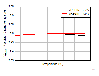
Figure 10. Regulator Output Voltage vs. Temperature
bq27530-G1 D003_SLUSBU6.gif
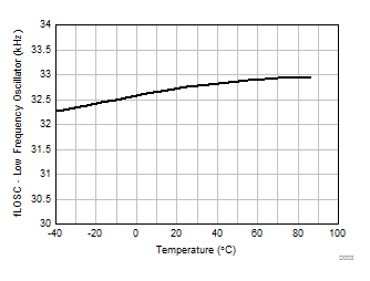
Figure 12. Low-Frequency Oscillator Frequency vs. Temperature
bq27530-G1 D002_SLUSBU6.gif
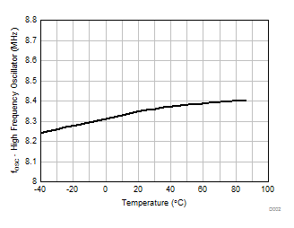
Figure 11. High-Frequency Oscillator Frequency vs. Temperature
bq27530-G1 D004_SLUSBU6.gif
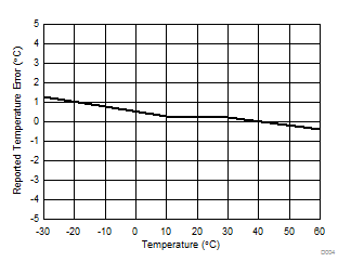
Figure 13. Reported Internal Temperature Measurement vs. Temperature