SLUSBU6B September 2014 – January 2016
PRODUCTION DATA.
- 1 Features
- 2 Applications
- 3 Description
- 4 Revision History
- 5 Pin Configuration and Functions
-
6 Specifications
- 6.1 Absolute Maximum Ratings
- 6.2 ESD Ratings
- 6.3 Recommended Operating Conditions
- 6.4 Thermal Information
- 6.5 Electrical Characteristics: Supply Current
- 6.6 Digital Input and Output DC Electrical Characteristics
- 6.7 Power-on Reset
- 6.8 2.5-V LDO Regulator
- 6.9 Internal Clock Oscillators
- 6.10 ADC (Temperature and Cell Measurement) Characteristics
- 6.11 Integrating ADC (Coulomb Counter) Characteristics
- 6.12 Data Flash Memory Characteristics
- 6.13 I2C-compatible Interface Communication Timing Requirements
- 6.14 Typical Characteristics
- 7 Detailed Description
- 8 Application and Implementation
- 9 Power Supply Recommendations
- 10Layout
- 11Device and Documentation Support
- 12Mechanical, Packaging, and Orderable Information
Package Options
Mechanical Data (Package|Pins)
- YZF|15
Thermal pad, mechanical data (Package|Pins)
Orderable Information
10 Layout
10.1 Layout Guidelines
10.1.1 Sense Resistor Connections
Kelvin connections at the sense resistor are just as critical as those for the battery terminals themselves. The differential traces should be connected at the inside of the sense resistor pads and not anywhere along the high-current trace path to prevent false increases to measured current that could result when measuring between the sum of the sense resistor and trace resistance between the tap points. In addition, the routing of these leads from the sense resistor to the input filter network and finally into the SRP and SRN pins needs to be as closely matched in length as possible else additional measurement offset could occur. It is further recommended to add copper trace or pour-based "guard rings" around the perimeter of the filter network and coulomb counter inputs to shield these sensitive pins from radiated EMI into the sense nodes. This prevents differential voltage shifts that could be interpreted as real current change to the fuel gauge. All of the filter components need to be placed as close as possible to the coulomb counter input pins.
10.1.2 Thermistor Connections
The thermistor sense input should include a ceramic bypass capacitor placed as close to the TS input pin as possible. The capacitor helps to filter measurements of any stray transients as the voltage bias circuit pulses periodically during temperature sensing windows.
10.1.3 High-Current and Low-Current Path Separation
For best possible noise performance, it is extremely important to separate the low-current and high-current loops to different areas of the board layout. The fuel gauge and all support components should be situated on one side of the boards and tap off of the high-current loop (for measurement purposes) at the sense resistor. Routing the low-current ground around instead of under high-current traces will further help to improve noise rejection.
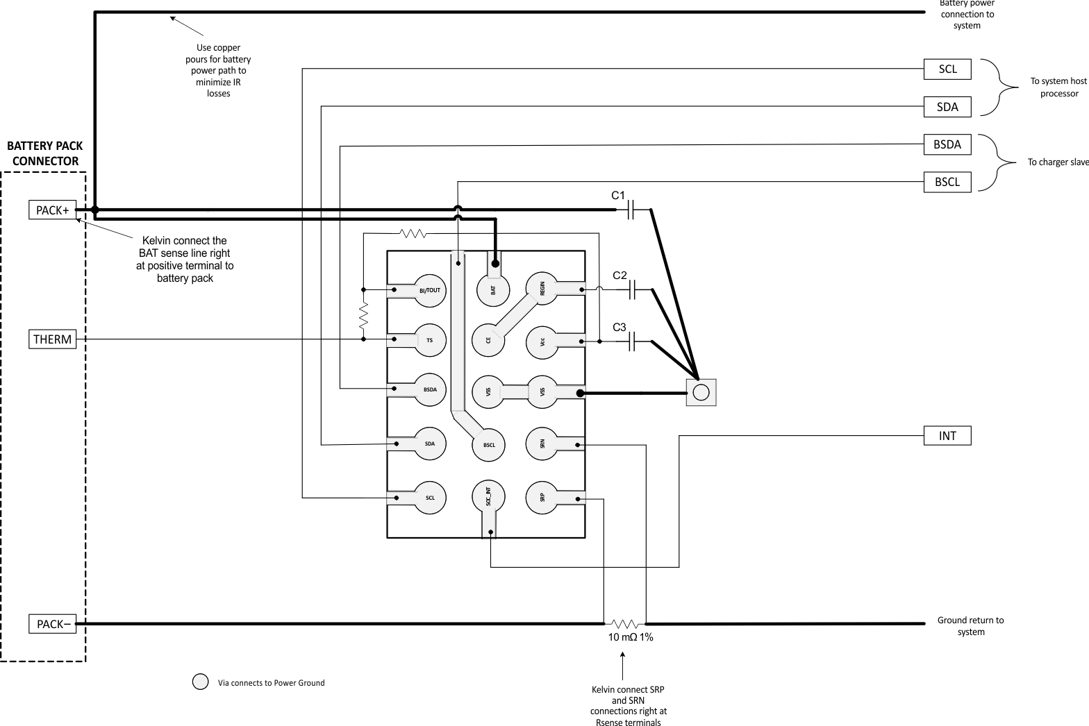
10.2 Layout Example
 Figure 17. bq27532-G1 Layout Schematic