SLUSFQ0 November   2024 BQ27Z758

PRODUCTION DATA  

  1.   1
  2. Features
  3. Applications
  4. Description
  5. Pin Configurations and Functions
  6. Specifications
    1. 5.1 Absolute Maximum Ratings
    2. 5.2 ESD Ratings
    3. 5.3 Recommended Operating Conditions
    4. 5.4 Thermal Information
    5. 5.5 Electrical Characteristics
      1. 5.5.1 Supply Current
      2. 5.5.2 Common Analog (LDO, LFO, HFO, REF1, REF2, I-WAKE)
      3. 5.5.3 Battery Protection (CHG, DSG)
      4. 5.5.4 Cell Sensing Output (BAT_SP, BAT_SN)
      5. 5.5.5 Gauge Measurements (ADC, CC, Temperature)
      6. 5.5.6 Flash Memory
    6. 5.6 Digital I/O: DC Characteristics
    7. 5.7 Digital I/O: Timing Characteristics
    8. 5.8 Typical Characteristics
  7. Detailed Description
    1. 6.1 Overview
    2. 6.2 Functional Block Diagram
    3. 6.3 Feature Description
      1. 6.3.1  BQ27Z758 Processor
      2. 6.3.2  Battery Parameter Measurements
        1. 6.3.2.1 Coulomb Counter (CC) and Digital Filter
        2. 6.3.2.2 ADC Multiplexer
        3. 6.3.2.3 Analog-to-Digital Converter (ADC)
        4. 6.3.2.4 Internal Temperature Sensor
        5. 6.3.2.5 External Temperature Sensor Support
      3. 6.3.3  Power Supply Control
      4. 6.3.4  ENAB Pin
      5. 6.3.5  Bus Communication Interface
      6. 6.3.6  Low Frequency Oscillator
      7. 6.3.7  High Frequency Oscillator
      8. 6.3.8  1.8-V Low Dropout Regulator
      9. 6.3.9  Internal Voltage References
      10. 6.3.10 Overcurrent in Discharge Protection
      11. 6.3.11 Overcurrent in Charge Protection
      12. 6.3.12 Short-Circuit Current in Discharge Protection
      13. 6.3.13 Primary Protection Features
      14. 6.3.14 Battery Sensing
      15. 6.3.15 Gas Gauging
      16. 6.3.16 Zero Volt Charging (ZVCHG)
      17. 6.3.17 Charge Control Features
      18. 6.3.18 Authentication
    4. 6.4 Device Functional Modes
      1. 6.4.1 Lifetime Logging Features
      2. 6.4.2 Configuration
        1. 6.4.2.1 Coulomb Counting
        2. 6.4.2.2 Cell Voltage Measurements
        3. 6.4.2.3 Auto Calibration
        4. 6.4.2.4 Temperature Measurements
  8. Applications and Implementation
    1. 7.1 Application Information
    2. 7.2 Typical Applications
      1. 7.2.1 Design Requirements (Default)
      2. 7.2.2 Detailed Design Procedure
        1. 7.2.2.1 Changing Design Parameters
      3. 7.2.3 Calibration Process
      4. 7.2.4 Gauging Data Updates
        1. 7.2.4.1 Application Curve
  9. Power Supply Requirements
  10. Layout
    1. 9.1 Layout Guidelines
    2. 9.2 Layout Example
  11. 10Device and Documentation Support
    1. 10.1 Third-Party Products Disclaimer
    2. 10.2 Documentation Support
      1. 10.2.1 Related Documentation
    3. 10.3 Receiving Notification of Documentation Updates
    4. 10.4 Support Resources
    5. 10.5 Trademarks
    6. 10.6 Electrostatic Discharge Caution
    7. 10.7 Glossary
  12. 11Revision History
  13. 12Mechanical, Orderable, and Packaging Information

Package Options

Refer to the PDF data sheet for device specific package drawings

Mechanical Data (Package|Pins)
  • YAH|15
Thermal pad, mechanical data (Package|Pins)
Orderable Information

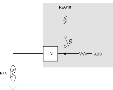
External Temperature Sensor Support

The TS input is enabled with an internal 18-kΩ (Typ.) linearization pull-up resistor to support the use of a 10-kΩ (25°C) NTC external thermistor, such as the Semitec 103AT-2. The NTC thermistor should be connected between VSS and the individual TS pin. The analog measurement is then taken by the ADC through its input multiplexer. If a different thermistor type is required, then changes to configurations may be required.
BQ27Z758 External Thermistor BiasingFigure 6-1 External Thermistor Biasing