SLUSB15J September 2012 – May 2021 BQ2947
PRODUCTION DATA
- 1 Features
- 2 Applications
- 3 Description
- 4 Revision History
- 5 Device Comparison Table
- 6 Pin Configuration and Functions
- 7 Specifications
- 8 Detailed Description
- 9 Application and Implementation
- 10Power Supply Recommendations
- 11Layout
- 12Device and Documentation Support
- 13Mechanical, Packaging, and Orderable Information
Package Options
Mechanical Data (Package|Pins)
- DSG|8
Thermal pad, mechanical data (Package|Pins)
- DSG|8
Orderable Information
8.3 Feature Description
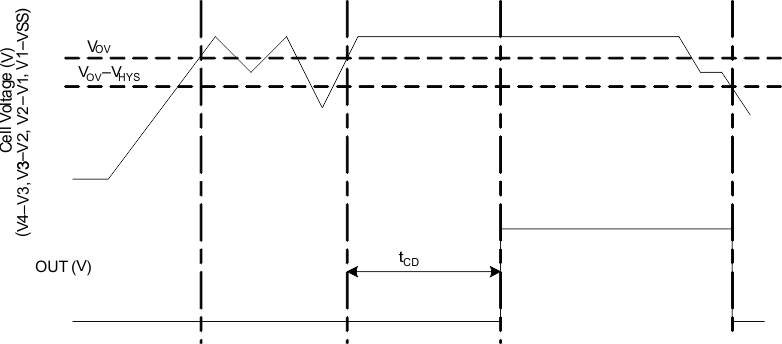
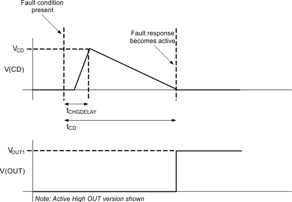
In the BQ2947 family of devices, if any cell voltage exceeds the programmed OV value, a timer circuit is activated. This timer circuit charges the CD pin to a nominal value, then slowly discharges it with a fixed current back down to VSS. When the CD pin falls below a nominal threshold near VSS, the OUT terminal goes from inactive to active state. Additionally, a timeout detection circuit checks to ensure that the CD pin successfully begins charging to above VSS and subsequently drops back down to VSS, and if a timeout error is detected in either direction, it will similarly trigger the OUT pin to become active. See Figure 8-2 for details on CD and OUT pin behavior during an overvoltage event.
For an NCH Open Drain Active Low configuration, the OUT pin pulls down to VSS when active (OV present) and is high impedance when inactive (no OV).
 Figure 8-1 Timing for Overvoltage Sensing (OUT Pin Is Active High)
Figure 8-2 shows the behavior of CD pin during an OV sequence.
 Figure 8-2 CD Pin Mechanism (OUT Pin Is Active High)
In the case of an Open Drain Active Low version, the VOUT signal will be high and transition to low state when the voltage on the VCD capacitor discharges to the set level based on the tCD timer.