SLUSBU5U November 2013 – October 2024 BQ2961 , BQ2962
PRODUCTION DATA
- 1
- 1 Features
- 2 Applications
- 3 Description
- 4 Device Comparison Table
- 5 Pin Configuration and Functions
- 6 Specifications
- 7 Detailed Description
- 8 Application and Implementation
- 9 Power Supply Recommendations
- 10Layout
- 11Device and Documentation Support
- 12Revision History
- 13Mechanical, Packaging, and Orderable Information
Package Options
Mechanical Data (Package|Pins)
- DSG|8
Thermal pad, mechanical data (Package|Pins)
- DSG|8
Orderable Information
7.3.3 Regulated Output Voltage and REG_EN Pin
For BQ2961, there are three factory-preprogrammed options for the regulated output voltage, 3.3 V, 2.5 V, and 1.8 V. For BQ2962, the regulated output voltage options are 3.3 V, 3.15 V, and 3.0 V. Potentially, the BQ2962xy device can provide other regulated voltage output between 3.3 V to 3.0 V. Contact Texas Instruments for details.
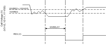
At power up, the regulated output is on by default. If any cell voltage is below VUVREG at device power up, the regulated output will remain on until the tUV_DELAY time has passed, the regulated output turns off after the delay time.
During discharge, if any cell voltage falls below the VUVREG threshold for tUV_DELAY time, the regulated output is self-disabled. The regulated output turns on again when all the cell voltages are above VUVREG + VUVHYS.
 Figure 7-2 REG Output Timing