SLUSBU5U November 2013 – October 2024 BQ2961 , BQ2962
PRODUCTION DATA
- 1
- 1 Features
- 2 Applications
- 3 Description
- 4 Device Comparison Table
- 5 Pin Configuration and Functions
- 6 Specifications
- 7 Detailed Description
- 8 Application and Implementation
- 9 Power Supply Recommendations
- 10Layout
- 11Device and Documentation Support
- 12Revision History
- 13Mechanical, Packaging, and Orderable Information
Package Options
Mechanical Data (Package|Pins)
- DSG|8
Thermal pad, mechanical data (Package|Pins)
- DSG|8
Orderable Information
8.2.2 Detailed Design Procedure
Note:
The device VSS must be connected first during PCB test or cell attachment. Failure to do so can damage the REG pin.
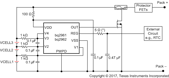
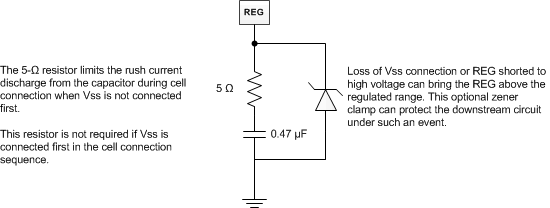
- If the VSS pin cannot be connected first, it is required to add a resistor of a minimum of 5 Ω to a maximum of 10 Ω (a 5-Ω resistor is used in the reference schematic, Figure 8-2) in series with the REG capacitor. When VSS is floating, the REG capacitor always charges up to the VDD voltage. When VSS is finally connected, the REG capacitor will be discharged. Adding a small resistor in series reduces the current strength and avoids any potential damage to the REG pin. The 5-Ω resistor can be placed in series with the REG connect circuit (as shown in Figure 8-2) or in series of the REG capacitor (as shown in Figure 8-3). Placing the resistor in series with the REG circuit results in a small drop of VREG (for example: max loading of IREG mA with a 5-Ω resistor will drop 5 mV on VREG), but such a connection can protect again rush current discharge from a REG capacitor or an external filter capacitor connected to the REG pin. Placing the resistor in series with the REG capacitor is an alternative to avoiding an additional drop in VREG if the filter capacitor used by the external circuit is much smaller than the REG capacitor.
- After VSS is connected, the device allows a random cell connection to the Vx pin.
- The cell should be connected to the lower Vn pin; the unused Vn pin should be shorted to the (Vn-1) pin. See Figure 8-2 for details.
 Figure 8-2 3-Series BQ2961 and BQ2962 Schematic
 - A Zener diode can be added to the REG pin to VSS,
as shown in Figure 8-3. This is recommended to protect the circuit
connected to the REG pin if floating VSS in the
field is a risk concern. When VSS is floating
(during cell connection when VSS is not connected
first or in a system fault with a broken BAT–
wire), the REG voltage always pulls up to VDD. In
a 4-series configuration, the REG voltage can
reach approximately 16 V with VSS floating. Adding
a Zener diode clamps the REG voltage to a safe
level for the external circuits connected to the
REG pin. Having the Zener diode can also protect
the external circuits if the REG pin is shorted to
the OUT pin or any other high-voltage output
terminal. If a Zener diode is used, TI recommends
putting the diode on the battery side with the
BQ296xxx device to allow protection on the REG
pin, as well as the circuit connected to REG under
the floating VSS condition. The resistor in series
with the REG pin is not required in this case.
 Figure 8-3 5-V
Zener Diode