SLUSBU5U
November 2013 – October 2024
BQ2961
,
BQ2962
PRODUCTION DATA
1
1
Features
2
Applications
3
Description
4
Device Comparison Table
5
Pin Configuration and Functions
6
Specifications
6.1
Absolute Maximum Ratings
6.2
ESD Ratings
6.3
Recommended Operating Conditions
6.4
Thermal Information
6.5
Electrical Characteristics
6.6
Typical Characteristics
7
Detailed Description
7.1
Overview
7.2
Functional Block Diagram
7.3
Feature Description
7.3.1
Pin Details
7.3.1.1
Input Sense Voltage, Vx
7.3.1.2
Output Drive, OUT
7.3.1.3
Supply Input, VDD
7.3.1.4
Regulated Supply Output, REG
7.3.2
Overvoltage Sensing for OUT
7.3.3
Regulated Output Voltage and REG_EN Pin
7.4
Device Functional Modes
7.4.1
NORMAL Mode
7.4.2
OVERVOLTAGE Mode
7.4.3
UNDERVOLTAGE Mode
7.4.4
CUSTOMER TEST MODE
8
Application and Implementation
8.1
Application Information
8.2
Typical Application
8.2.1
Design Requirements
8.2.2
Detailed Design Procedure
8.2.3
Application Curves
9
Power Supply Recommendations
10
Layout
10.1
Layout Guidelines
10.2
Layout Example
11
Device and Documentation Support
11.1
Third-Party Products Disclaimer
11.2
Receiving Notification of Documentation Updates
11.3
Support Resources
11.4
Trademarks
11.5
Electrostatic Discharge Caution
11.6
Glossary
12
Revision History
13
Mechanical, Packaging, and Orderable Information
Package Options
Mechanical Data (Package|Pins)
DSG|8
MPDS308C
Thermal pad, mechanical data (Package|Pins)
DSG|8
QFND141I
Orderable Information
slusbu5u_oa
slusbu5u_pm
8.2.3
Application Curves
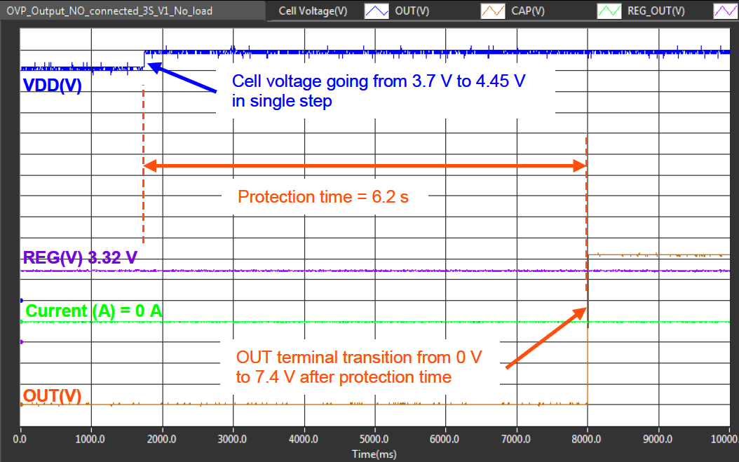
Figure 8-4
Overvoltage Protection
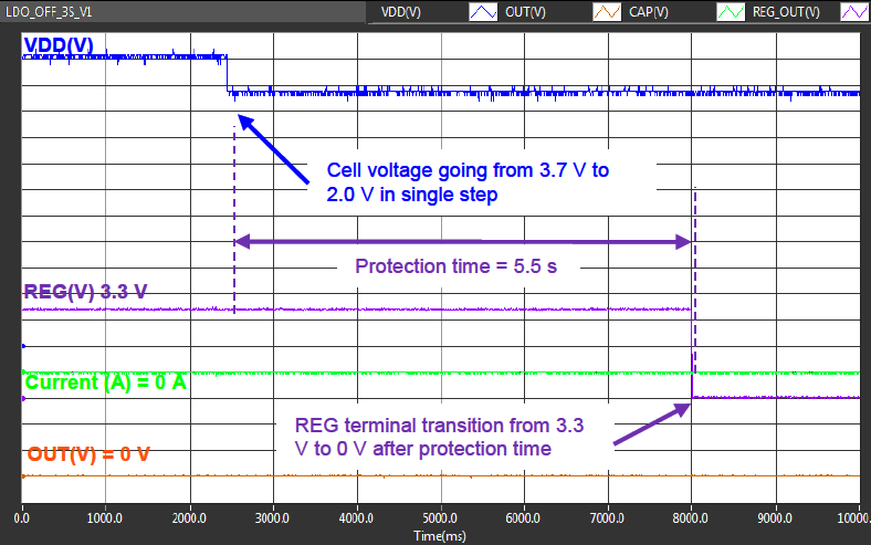
Figure 8-6
Undervoltage Detection to Turn Off the Regulator
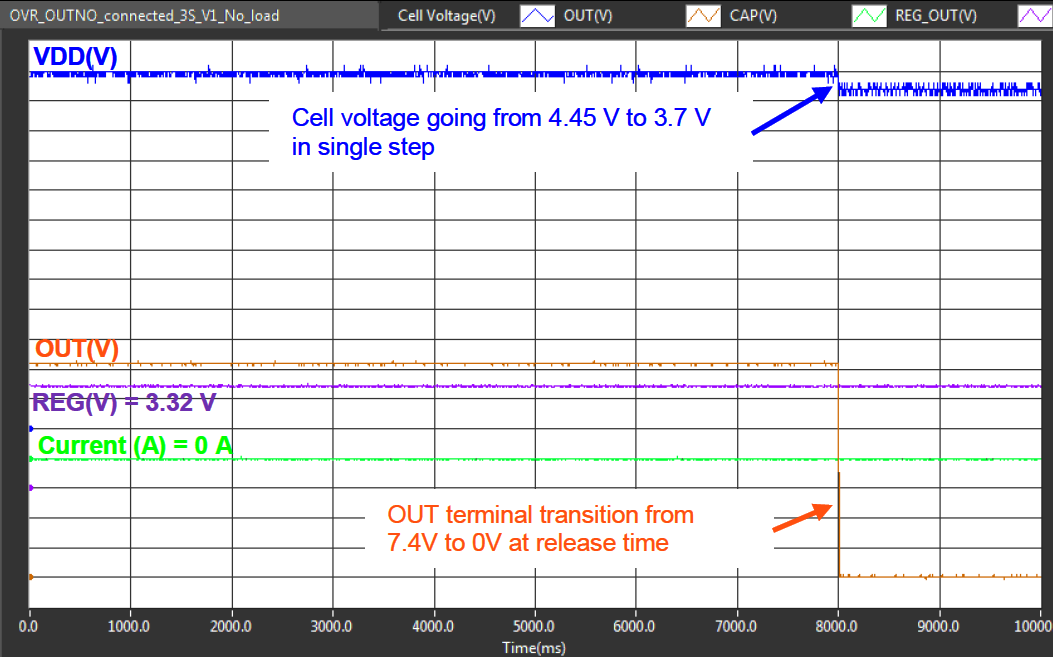
Figure 8-5
Overvoltage Protection Release
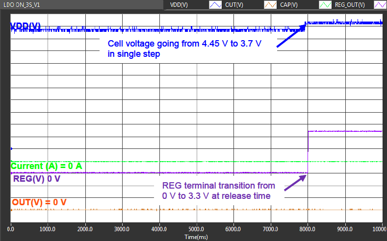
Figure 8-7
Undervoltage Release to Switch On the Regulator