SLUSBU5U November 2013 – October 2024 BQ2961 , BQ2962
PRODUCTION DATA
- 1
- 1 Features
- 2 Applications
- 3 Description
- 4 Device Comparison Table
- 5 Pin Configuration and Functions
- 6 Specifications
- 7 Detailed Description
- 8 Application and Implementation
- 9 Power Supply Recommendations
- 10Layout
- 11Device and Documentation Support
- 12Revision History
- 13Mechanical, Packaging, and Orderable Information
Package Options
Mechanical Data (Package|Pins)
- DSG|8
Thermal pad, mechanical data (Package|Pins)
- DSG|8
Orderable Information
3 Description
The BQ296xxx family is a high-accuracy, low-power overvoltage protector with a 2mA regulated output supply for Li-ion battery pack applications.
Each cell in a 2-series to 4-series cell stack is individually monitored for an overvoltage condition. An internally fixed-delay timer is initiated upon detection of an overvoltage condition on any cell. Upon expiration of the delay timer, an output pin is triggered into an active state to indicate that an overvoltage condition has occurred.
The regulated output supply delivers up to 2mA (max) output current to drive always-on circuits, such as a real-time clock (RTC) oscillator. The BQ296xxx family has a self-disable function to turn off the regulated output if any cell voltage falls below a certain threshold, thereby preventing drain on the battery, and provides an external control to enable or disable the regulated output.
| PART NUMBER | PACKAGE (1) | BODY SIZE (NOM) |
|---|---|---|
| BQ2961 | WSON (8) | 2.00mm × 2.00mm |
| BQ2962 |
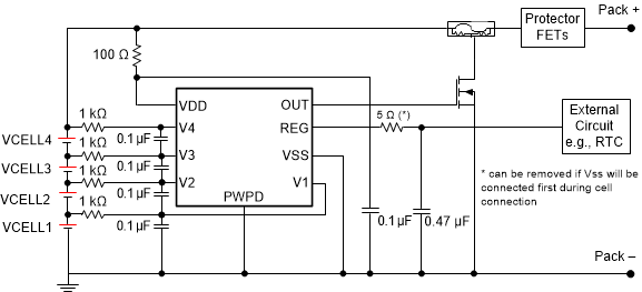
 Simplified Schematic