SLUSBU5U November 2013 – October 2024 BQ2961 , BQ2962
PRODUCTION DATA
- 1
- 1 Features
- 2 Applications
- 3 Description
- 4 Device Comparison Table
- 5 Pin Configuration and Functions
- 6 Specifications
- 7 Detailed Description
- 8 Application and Implementation
- 9 Power Supply Recommendations
- 10Layout
- 11Device and Documentation Support
- 12Revision History
- 13Mechanical, Packaging, and Orderable Information
Package Options
Mechanical Data (Package|Pins)
- DSG|8
Thermal pad, mechanical data (Package|Pins)
- DSG|8
Orderable Information
5 Pin Configuration and Functions
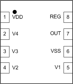
 Figure 5-1 2-Series to 4-Series BQ2961(Top View)
 Figure 5-2 2-Series to 4-Series BQ2962(Top View)
Table 5-1 Pin Functions
| PIN | TYPE(1) | DESCRIPTION | ||
|---|---|---|---|---|
| NAME | BQ2961 | BQ2962 | ||
| OUT | 8 | 7 | OA | Analog output drive for an overvoltage fault signal; CMOS output high or open-drain active low |
| PWPD | 9 | 9 | P | TI recommends connecting the exposed pad to VSS on PCB. |
| REG | 7 | 8 | OA | Regulated supply output. Requires an external ceramic capacitor for stability |
| REG_EN | — | — | IA | Regulated supply output enable. A "high" to enable REG output and "low" to disable REG output |
| V1 | 5 | 5 | IA | Sense input for positive voltage of the lowest cell from the bottom of the stack |
| V2 | 4 | 4 | IA | Sense input for positive voltage of the second cell from the bottom of the stack |
| V3 | 3 | 3 | IA | Sense input for positive voltage of the third cell from the bottom of the stack |
| V4 | 2 | 2 | IA | Sense input for positive voltage of the fourth cell from the bottom of the stack |
| VDD | 1 | 1 | P | Power supply input |
| VSS | 6 | 6 | P | Electrically connected to integrated circuit ground and negative terminal of the lowest cell in the stack |
(1) IA = Analog input, OA = Analog
Output, P = Power connection