SLUSBU5U November 2013 – October 2024 BQ2961 , BQ2962
PRODUCTION DATA
- 1
- 1 Features
- 2 Applications
- 3 Description
- 4 Device Comparison Table
- 5 Pin Configuration and Functions
- 6 Specifications
- 7 Detailed Description
- 8 Application and Implementation
- 9 Power Supply Recommendations
- 10Layout
- 11Device and Documentation Support
- 12Revision History
- 13Mechanical, Packaging, and Orderable Information
Package Options
Mechanical Data (Package|Pins)
- DSG|8
Thermal pad, mechanical data (Package|Pins)
- DSG|8
Orderable Information
7.4.4 CUSTOMER TEST MODE
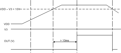
The Customer Test Mode (CTM) helps to reduce test time for checking the overvoltage delay-timer parameter once the circuit is implemented into the battery pack. To enter CTM, the VDD pin should be set at least 10 V higher than V3 (see Figure 7-3). The delay timer is greater than 10 ms, but considerably shorter than the timer delay in normal operation. To exit CTM, remove the VDD to VC3 voltage differential of 10 V, so that the decrease in the value automatically causes an exit.
Avoid exceeding any Absolute Maximum Voltages on any pins when placing the device into CTM. Also avoid exceeding Absolute Maximum Voltages for the individual cell voltages (V3–V2), (V2–V1) and (V1–VSS). Stressing the pins beyond the rated limits can cause permanent damage to the device.
Figure 7-3 shows the timing for the Customer Test Mode.
 Figure 7-3 Timing for Customer Test Mode
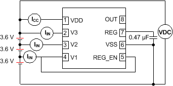
Figure 7-4 shows the measurement for current consumption of the product for both VDD and Vx.
 Figure 7-4 Configuration for Integrated Circuit Current Consumption Test