SLUSBU9I March   2014  – August 2024 BQ2970 , BQ2971 , BQ2972 , BQ2973

PRODUCTION DATA  

  1.   1
  2. Features
  3. Applications
  4. Description
  5. Device Comparison Table
  6. Pin Configuration and Functions
    1. 5.1 Pin Descriptions
      1. 5.1.1 Supply Input: BAT
      2. 5.1.2 Cell Negative Connection: VSS
      3. 5.1.3 Voltage Sense Node: V–
      4. 5.1.4 Discharge FET Gate Drive Output: DOUT
      5. 5.1.5 Charge FET Gate Drive Output: COUT
  7. Specifications
    1. 6.1 Absolute Maximum Ratings
    2. 6.2 ESD Ratings
    3. 6.3 Recommended Operating Conditions
    4. 6.4 Thermal Information
    5. 6.5 DC Characteristics
    6. 6.6 Programmable Fault Detection Thresholds
    7. 6.7 Programmable Fault Detection Timer Ranges
    8. 6.8 Typical Characteristics
  8. Parameter Measurement Information
    1. 7.1 Timing Charts
    2. 7.2 Test Circuits
    3. 7.3 Test Circuit Diagrams
  9. Detailed Description
    1. 8.1 Overview
    2. 8.2 Functional Block Diagram
    3. 8.3 Feature Description
    4. 8.4 Device Functional Modes
      1. 8.4.1 Normal Operation
      2. 8.4.2 Overcharge Status
      3. 8.4.3 Over-Discharge Status
      4. 8.4.4 Discharge Overcurrent Status (Discharge Overcurrent, Load Short-Circuit)
      5. 8.4.5 Charge Overcurrent Status
      6. 8.4.6 0V Charging Function Enabled
      7. 8.4.7 0V Charging Inhibit Function
      8. 8.4.8 Delay Circuit
  10. Application and Implementation
    1. 9.1 Application Information
    2. 9.2 Typical Application
      1. 9.2.1 Design Requirements
      2. 9.2.2 Detailed Design Procedure
      3. 9.2.3 Application Performance Plots
    3. 9.3 Power Supply Recommendations
    4. 9.4 Layout
      1. 9.4.1 Layout Guidelines
      2. 9.4.2 Layout Example
  11. 10Device and Documentation Support
    1. 10.1 Related Documentation
    2. 10.2 Support Resources
    3. 10.3 Trademarks
    4. 10.4 Electrostatic Discharge Caution
    5. 10.5 Glossary
  12. 11Revision History
  13. 12Mechanical, Packaging, and Orderable Information

Package Options

Mechanical Data (Package|Pins)
Thermal pad, mechanical data (Package|Pins)
Orderable Information

Application Performance Plots

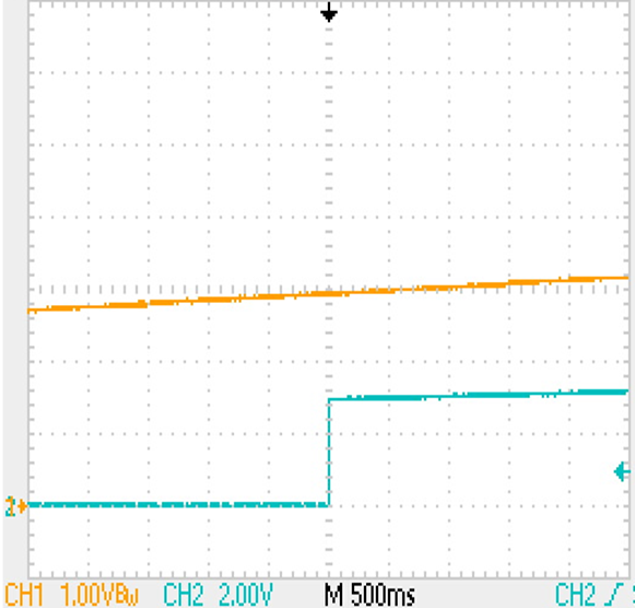
BQ2970 BQ2971 BQ2972 BQ2973 UVP
                        Recovery
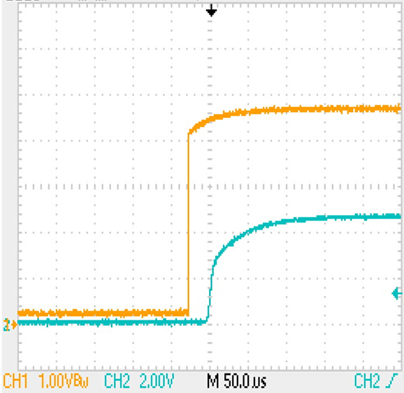
Orange Line (Channel 1) = Power Up Ramp on BAT Pin
Turquoise Line (Channel 2) = DOUT Gate Drive Output
DOUT goes from low to high when UVP Recovery = UVP Set Threshold +100mV
Figure 9-2 UVP Recovery
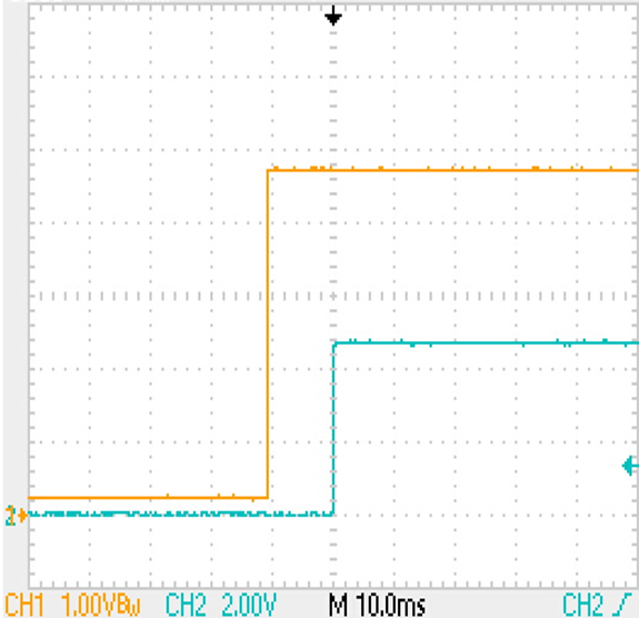
BQ2970 BQ2971 BQ2972 BQ2973 Initial Power Up, DOUT
Orange Line (Channel 1) = Power Up Ramp on BAT pin
Turquoise Line (Channel 2) = DOUT Gate Drive Output
Figure 9-4 Initial Power Up, DOUT
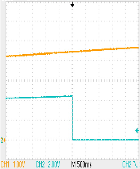
BQ2970 BQ2971 BQ2972 BQ2973 OVP
                        Set Condition
Orange Line (Channel 1) = Power Up Ramp on BAT Pin
Turquoise Line (Channel 2) = COUT Gate Drive Output
COUT goes from high to low when OVP threshold = OVP set Threshold + set delay time
Figure 9-6 OVP Set Condition
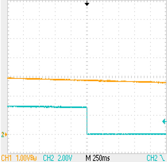
BQ2970 BQ2971 BQ2972 BQ2973 UVP
                        Set Condition
Orange Line (Channel 1) = Power Down Ramp on BAT Pin
Turquoise Line (Channel 2) = DOUT Date Drive Output
DOUT goes from high to low when UVP threshold = UVP set Threshold + set delay time
Figure 9-3 UVP Set Condition
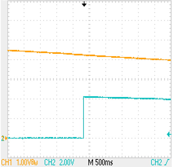
BQ2970 BQ2971 BQ2972 BQ2973 Initial Power Up, COUT
Orange Line (Channel 1) = Power Up Ramp on BAT Pin
Turquoise Line (Channel 2) = COUT Gate Drive Output
Figure 9-5 Initial Power Up, COUT
BQ2970 BQ2971 BQ2972 BQ2973 OVP Recovery Condition
Orange Line (Channel 1) = Decrease Voltage on BAT Pin
Turquoise Line (Channel 2) = COUT Gate Drive Output
COUT goes from low to high when OVP Recovery = OVP Set Threshold –100mV
Figure 9-7 OVP Recovery Condition