SLUSBU9I March   2014  – August 2024 BQ2970 , BQ2971 , BQ2972 , BQ2973

PRODUCTION DATA  

  1.   1
  2. Features
  3. Applications
  4. Description
  5. Device Comparison Table
  6. Pin Configuration and Functions
    1. 5.1 Pin Descriptions
      1. 5.1.1 Supply Input: BAT
      2. 5.1.2 Cell Negative Connection: VSS
      3. 5.1.3 Voltage Sense Node: V–
      4. 5.1.4 Discharge FET Gate Drive Output: DOUT
      5. 5.1.5 Charge FET Gate Drive Output: COUT
  7. Specifications
    1. 6.1 Absolute Maximum Ratings
    2. 6.2 ESD Ratings
    3. 6.3 Recommended Operating Conditions
    4. 6.4 Thermal Information
    5. 6.5 DC Characteristics
    6. 6.6 Programmable Fault Detection Thresholds
    7. 6.7 Programmable Fault Detection Timer Ranges
    8. 6.8 Typical Characteristics
  8. Parameter Measurement Information
    1. 7.1 Timing Charts
    2. 7.2 Test Circuits
    3. 7.3 Test Circuit Diagrams
  9. Detailed Description
    1. 8.1 Overview
    2. 8.2 Functional Block Diagram
    3. 8.3 Feature Description
    4. 8.4 Device Functional Modes
      1. 8.4.1 Normal Operation
      2. 8.4.2 Overcharge Status
      3. 8.4.3 Over-Discharge Status
      4. 8.4.4 Discharge Overcurrent Status (Discharge Overcurrent, Load Short-Circuit)
      5. 8.4.5 Charge Overcurrent Status
      6. 8.4.6 0V Charging Function Enabled
      7. 8.4.7 0V Charging Inhibit Function
      8. 8.4.8 Delay Circuit
  10. Application and Implementation
    1. 9.1 Application Information
    2. 9.2 Typical Application
      1. 9.2.1 Design Requirements
      2. 9.2.2 Detailed Design Procedure
      3. 9.2.3 Application Performance Plots
    3. 9.3 Power Supply Recommendations
    4. 9.4 Layout
      1. 9.4.1 Layout Guidelines
      2. 9.4.2 Layout Example
  11. 10Device and Documentation Support
    1. 10.1 Related Documentation
    2. 10.2 Support Resources
    3. 10.3 Trademarks
    4. 10.4 Electrostatic Discharge Caution
    5. 10.5 Glossary
  12. 11Revision History
  13. 12Mechanical, Packaging, and Orderable Information

Package Options

Mechanical Data (Package|Pins)
Thermal pad, mechanical data (Package|Pins)
Orderable Information

Typical Characteristics

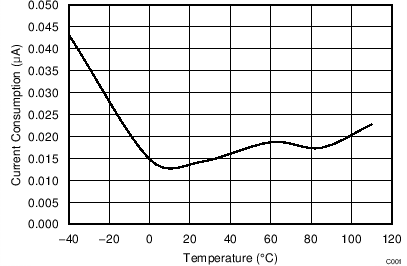
BQ2970 BQ2971 BQ2972 BQ2973 1.5V
                            IBAT Versus Temperature
VBAT = 1.5V
Figure 6-1 1.5V IBAT Versus Temperature
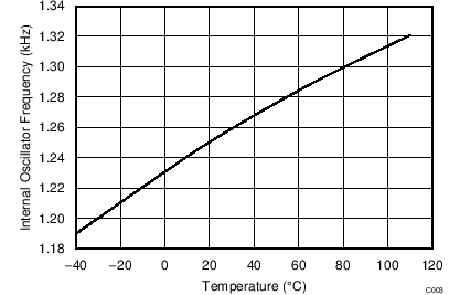
BQ2970 BQ2971 BQ2972 BQ2973 Internal Oscillator Frequency Versus Temperature
FOSC, Setting = 1.255kHz
Figure 6-3 Internal Oscillator Frequency Versus Temperature
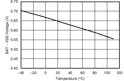
BQ2970 BQ2971 BQ2972 BQ2973 0V
                        Charging Disallowed Versus Temperature
Figure 6-5 0V Charging Disallowed Versus Temperature
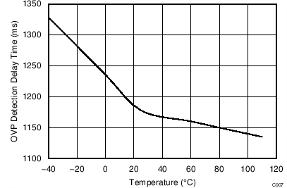
BQ2970 BQ2971 BQ2972 BQ2973 OVP Detection Dely Time Versus Temperature
tOVPD, Setting = 1.25s
Figure 6-7 OVP Detection Dely Time Versus Temperature
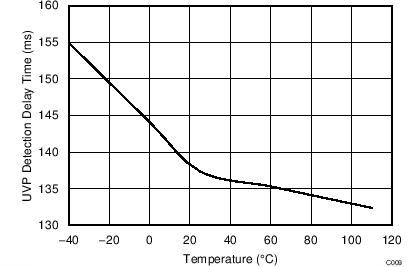
BQ2970 BQ2971 BQ2972 BQ2973 UVP Detection Delay Time Versus Temperature
tUVPD, Setting = 144ms
Figure 6-9 UVP Detection Delay Time Versus Temperature
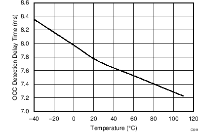
BQ2970 BQ2971 BQ2972 BQ2973 OCC Detection Delay Time Versus Temperature
tOCCD, Setting = 8ms
Figure 6-11 OCC Detection Delay Time Versus Temperature
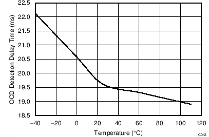
BQ2970 BQ2971 BQ2972 BQ2973 OCD Detection Delay Time Versus Temperature
tUVPD, Setting = 20ms
Figure 6-13 OCD Detection Delay Time Versus Temperature
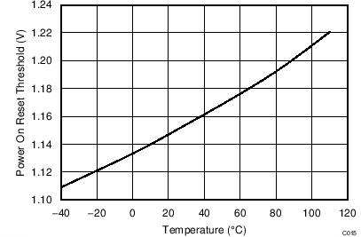
BQ2970 BQ2971 BQ2972 BQ2973 Power On Reset Versus Temperature
Figure 6-15 Power On Reset Versus Temperature
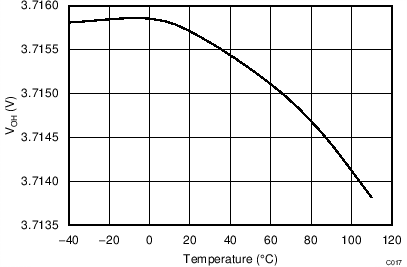
BQ2970 BQ2971 BQ2972 BQ2973 DOUT Versus Temperature
                        with Ioh =
                        –30µA
VBAT, Setting = 3.9V
Figure 6-17 DOUT Versus Temperature with Ioh = –30µA
BQ2970 BQ2971 BQ2972 BQ2973 3.9V
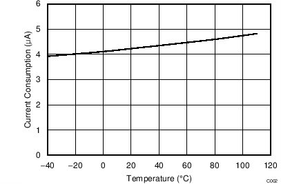
                            IBAT Versus Temperature
VBAT = 3.9V
Figure 6-2 3.9V IBAT Versus Temperature
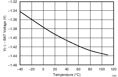
BQ2970 BQ2971 BQ2972 BQ2973 0V
                        Charging Allowed Versus Temperature
VBAT, Setting = 0V
Figure 6-4 0V Charging Allowed Versus Temperature
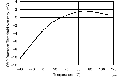
BQ2970 BQ2971 BQ2972 BQ2973 OVP Detection Accuracy Versus Temperature
OVP, Setting = 4.275V
Figure 6-6 OVP Detection Accuracy Versus Temperature
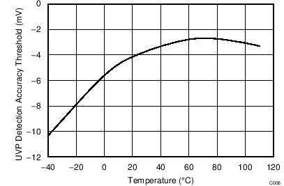
BQ2970 BQ2971 BQ2972 BQ2973 UVP Detection Accuracy Versus Temperature
UVP, Setting = 2.800V
Figure 6-8 UVP Detection Accuracy Versus Temperature
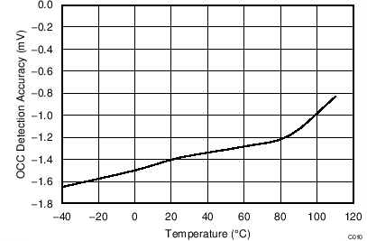
BQ2970 BQ2971 BQ2972 BQ2973 OCC Detection Accuracy Versus Temperature
VOCC, Setting = –100mV
Figure 6-10 OCC Detection Accuracy Versus Temperature
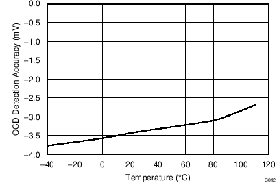
BQ2970 BQ2971 BQ2972 BQ2973 OCD Detection Accuracy Versus Temperature
VOCD, Setting = 100mV
Figure 6-12 OCD Detection Accuracy Versus Temperature
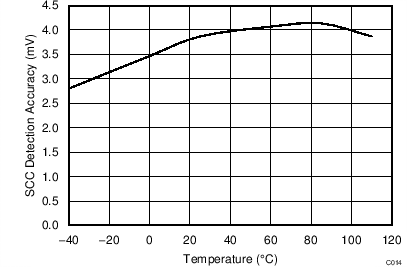
BQ2970 BQ2971 BQ2972 BQ2973 SCC Detection Accuracy Versus Temperature
VSCC, Setting = 500mV
Figure 6-14 SCC Detection Accuracy Versus Temperature
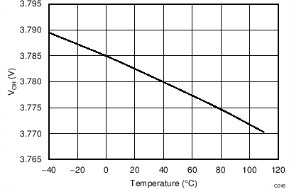
BQ2970 BQ2971 BQ2972 BQ2973 COUT Versus Temperature
                        with Ioh =
                        –30µA
VBAT, Setting = 3.9V
Figure 6-16 COUT Versus Temperature with Ioh = –30µA