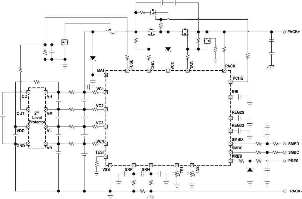
The bq3055 device is a fully integrated, single-chip, pack-based solution that provides a rich array of features for gas gauging, protection, and authentication for 2-series, 3-series, and 4-series cell Li-Ion and Li-Polymer battery packs.
Using its integrated high-performance analog peripherals, the bq3055 device measures and maintains an accurate record of available capacity, voltage, current, temperature, and other critical parameters in Li-Ion or Li-Polymer batteries, and reports this information to the system host controller over an SMBus v1.1 compatible interface.
The bq3055 provides software-based 1st-level and 2nd-level safety protection for overvoltage, undervoltage, overtemperature, and overcharge conditions, as well as hardware-based protection for overcurrent in discharge and short circuit in charge and discharge conditions.
SHA-1 authentication with secure memory for authentication keys enables identification of genuine battery packs beyond any doubt.
The compact 30-lead TSSOP package minimizes solution cost and size for smart batteries while providing maximum functionality and safety for battery gauging applications.
PART NUMBER | PACKAGE | BODY SIZE (NOM) |
---|---|---|
bq3055 | TSSOP (30) | 7.80 mm × 4.40 mm |
Changes from B Revision (October 2013) to C Revision
Changes from A Revision (June 2011) to B Revision
PIN | TYPE(1) | DESCRIPTION | |
---|---|---|---|
NAME | NO. | ||
BAT | 2 | P | Alternate power source |
CHG | 1 | O | Charge N-FET gate drive |
DSG | 30 | O | Discharge N-FET gate drive |
FUSE | 26 | O | Fuse drive |
NC | 14 | — | Not internally connected. Connect to VSS. |
NC | 16 | — | Not internally connected. Connect to VSS. |
NC | 17 | — | Not internally connected. Connect to VSS. |
NC | 18 | — | Not internally connected. Connect to VSS. |
NC | 19 | — | Not internally connected. Connect to VSS. |
NC | 20 | — | Not internally connected. Connect to VSS. |
PACK | 29 | P | Alternate power source |
PCHG | 28 | I/OD | Precharge P-FET gate drive |
PRES | 12 | I | Host system present input |
RBI | 21 | P | RAM backup |
REG25 | 22 | P | 2.5-V regulator output |
REG33 | 24 | P | 3.3-V regulator output |
SMBC | 15 | I/OD | SMBus v1.1 clock line |
SMBD | 13 | I/OD | SMBus v1.1 data line |
SRN | 10 | AI | Differential Coulomb Counter input |
SRP | 9 | AI | Differential Coulomb Counter input |
TEST | 25 | — | Test pin, connect to VSS through 2-kΩ resistor. |
TS1 | 8 | AI | Temperature sensor 1 thermistor input |
TS2 | 11 | AI | Temperature sensor 2 thermistor input |
VC1 | 3 | I | Sense input for positive voltage of top most cell in stack and cell balancing input for top most cell in stack |
VC2 | 4 | I | Sense input for positive voltage of third lowest cell in stack and cell balancing input for third lowest cell in stack |
VC3 | 5 | I | Sense input for positive voltage of second lowest cell in stack and cell balancing input for second lowest cell in stack |
VC4 | 6 | I | Sense input for positive voltage of lowest cell in stack and cell balancing input for lowest cell in stack |
VCC | 27 | P | Power supply voltage |
VSS | 7 | P | Device ground |
VSS | 23 | P | Device ground |
VALUE | UNIT | ||||
---|---|---|---|---|---|
V(ESD) | Electrostatic discharge | Human body model (HBM), per ANSI/ESDA/JEDEC JS-001(1) | All pins except pins 3 to 6 | ±2000 | V |
Pins 3 to 6 | ±1000 | ||||
Charged device model (CDM), per JEDEC specification JESD22-C101(2) | ±500 |
MIN | NOM | MAX | UNIT | ||||
---|---|---|---|---|---|---|---|
Supply voltage | VCC, PACK | 25 | V | ||||
BAT | 3.8 | VVC2 + 5 | |||||
VSTARTUP | Start up voltage at PACK | 3 | 5.5 | V | |||
VIN | Input voltage range | VC1, BAT | VVC2 | VVC2 + 5 | V | ||
VC2 | VVC3 | VVC3 + 5 | |||||
VC3 | VVC4 | VVC4 + 5 | |||||
VC4 | VSRP | VSRP + 5 | |||||
VCn – VC(n+1), (n=1, 2, 3, 4) | 0 | 5 | |||||
PACK | 25 | ||||||
SRP to SRN | –0.2 | 0.2 | |||||
CREG33 | External 3.3-V REG capacitor | 1 | µF | ||||
CREG25 | External 2.5-V REG capacitor | 1 | µF | ||||
TOPR | Operating temperature | –40 | 85 | °C |
THERMAL METRIC(1) | bq3055 | UNIT | |
---|---|---|---|
TSSOP (DBT) | |||
30 PINS | |||
RθJA | Junction-to-ambient thermal resistance | 73.1 | °C/W |
RθJC(top) | Junction-to-case(top) thermal resistance | 17.5 | °C/W |
RθJB | Junction-to-board thermal resistance | 34.5 | °C/W |
ψJT | Junction-to-top characterization parameter | 0.3 | °C/W |
ψJB | Junction-to-board characterization parameter | 30.3 | °C/W |
RθJC(bot) | Junction-to-case(bottom) thermal resistance | n/a | °C/W |
PARAMETER | TEST CONDITIONS | MIN | TYP | MAX | UNIT | |
---|---|---|---|---|---|---|
ICC | Normal | CHG on, DSG on, no Flash write | 410 | µA | ||
Sleep | CHG on, DSG on, no SBS communication | 160 | ||||
CHG off, DSG off, no SBS communication | 80 | |||||
Shutdown | 3.7 |
PARAMETER | TEST CONDITIONS | MIN | TYP | MAX | UNIT | |
---|---|---|---|---|---|---|
VIT– | Negative-going voltage input | At REG25 | 1.9 | 2 | 2.1 | V |
VHYS | POR Hysteresis | At REG25 | 65 | 125 | 165 | mV |
PARAMETER | TEST CONDITIONS | MIN | TYP | MAX | UNIT | |
---|---|---|---|---|---|---|
VWAKE | VWAKE Threshold | VWAKE | 0.2 | 1.2 | 2 | mV |
VWAKE | 0.4 | 2.4 | 3.6 | |||
VWAKE | 2 | 5 | 6.8 | |||
VWAKE | 5.3 | 10 | 13 | |||
VWAKE_TCO | Temperature drift of VWAKE accuracy | 0.5% | °C | |||
tWAKE | Time from application of current and wake of bq3055 | 0.2 | 1 | ms |
PARAMETER | TEST CONDITIONS | MIN | TYP | MAX | UNIT | |
---|---|---|---|---|---|---|
I(RBI) | RBI data-retention input current | VRBI > V(RBI)MIN, VCC < VIT | 20 | 1100 | nA | |
VRBI > V(RBI)MIN, VCC < VIT, TA= 0°C to 70°C |
500 | |||||
V(RBI) | RBI data-retention voltage | 1 | V |
PARAMETER | TEST CONDITIONS | MIN | TYP | MAX | UNIT | |
---|---|---|---|---|---|---|
VREG33 | Regulator output voltage | 3.8 V < VCC or BAT ≤ 5 V, ICC ≤4 mA |
2.4 | 3.5 | V | |
5V < VCC or BAT ≤ 6.8 V, ICC ≤13 mA |
3.1 | 3.3 | 3.5 | |||
6.8 V < VCC or BAT ≤ 20 V, ICC ≤ 30 mA |
3.1 | 3.3 | 3.5 | |||
IREG33 | Regulator output current | 2 | mA | |||
ΔV(VDDTEMP) | Regulator output change with temperature | VCC or BAT = 14.4 V, IREG33 = 2 mA | 0.2% | |||
ΔV(VDDLINE) | Line regulation | VCC or BAT = 14.4 V, IREG33 = 2 mA | 1 | 13 | mV | |
ΔV(VDDLOAD) | Load regulation | VCC or BAT = 14.4 V, IREG33 = 2 mA | 5 | 18 | mV | |
I(REG33MAX) | Current limit | VCC or BAT = 14.4 V, VREG33 = 3 V | 70 | mA | ||
VCC or BAT = 14.4 V, VREG33 = 0 V | 33 |
PARAMETER | TEST CONDITIONS | MIN | TYP | MAX | UNIT | |
---|---|---|---|---|---|---|
VREG25 | Regulator output voltage | IREG25 = 10 mA | 2.35 | 2.5 | 2.55 | V |
IREG25 | Regulator output current | 3 | mA | |||
ΔV(VDDTEMP) | Regulator output change with temperature | VCC or BAT = 14.4 V, IREG25 = 2 mA | 0.25% | |||
ΔV(VDDLINE) | Line regulation | VCC or BAT = 14.4 V, IREG25 = 2 mA | 1 | 4 | mV | |
ΔV(VDDLOAD) | Load regulation | VCC or BAT = 14.4 V, IREG25 = 2 mA | 20 | 40 | mV | |
I(REG33MAX) | Current limit | VCC or BAT = 14.4 V, VREG25 = 2.3 V | 65 | mA | ||
VCC or BAT = 14.4 V, VREG25 = 0 V | 23 |
PARAMETER | TEST CONDITIONS | MIN | TYP | MAX | UNIT | |
---|---|---|---|---|---|---|
VIH | High-level input | PRES, SMBD, SMBC | 2.0 | V | ||
VIL | Low-level input | PRES, SMBD, SMBC | 0.8 | V | ||
VOL | Low-level output voltage | SMBD, SMBC | 0.4 | V | ||
CIN | Input capacitance | PRES, SMBD, SMBC | 5 | pF | ||
ILKG | Input leakage current | PRES, SMBD, SMBC | 1 | μA | ||
IWPU | Weak pullup current | PRES, VOH = VREG25 – 0.5 V | 60 | 120 | μA | |
RPD(SMBx) | SMBC, SMBD pulldown | TA = –40 to 100˚C | 550 | 775 | 1000 | kΩ |
PARAMETER | TEST CONDITIONS | MIN | TYP | MAX | UNIT | |
---|---|---|---|---|---|---|
V(FETON) | Output voltage, charge, and discharge FETs on | VO(FETONDSG) = V(DSG) – VPACK, VGS connect 10 MΩ, VCC 3.8 V to 8.4 V | 8 | 9.7 | 12 | V |
VO(FETONDSG) = V(DSG) – VPACK, VGS connect 10 MΩ, VCC > 8.4 V | 9 | 11 | 12 | |||
VO(FETONCHG) = V(CHG) – VBAT, VGS connect 10 MΩ, VCC 3.8 V to 8.4 V | 8 | 9.7 | 12 | |||
VO(FETONCHG) = V(CHG) – VBAT, VGS connect 10 MΩ, VCC > 8.4 V | 9 | 11 | 12 | |||
V(FETOFF) | Output voltage, charge and discharge FETs off | VO(FETOFFDSG) = V(DSG) – VPACK | –0.4 | 0.4 | V | |
VO(FETOFFCHG) = V(CHG) – VBAT | –0.4 | 0.4 | ||||
tr | Rise time | CL= 4700 pF RG= 5.1 kΩ VCC < 8.4 VDSG: VBAT to VBAT + 4 V VCHG: VPACK to VPACK + 4 V |
800 | 1400 | μs | |
CL = 4700 pF RG = 5.1 kΩ VCC > 8.4 VDSG: VBAT to VBAT + 4 V VCHG: VPACK to VPACK + 4 V |
200 | 500 | ||||
tf | Fall time | CL = 4700 pF RG = 5.1 kΩ VDSG: VBAT + VO(FETONDSG) to VBAT + 1 V VCHG: VPACK + VO(FETONCHG) to VPACK + 1 V |
80 | 200 | μs |
PARAMETER | TEST CONDITIONS | MIN | TYP | MAX | UNIT | |
---|---|---|---|---|---|---|
VPU_PCHG | PCHG pullup voltage | VCC | V | |||
VOL_PCHG | PCHG output voltage low | IOL = 1 mA | 0.3 | V |
PARAMETER | TEST CONDITIONS | MIN | TYP | MAX | UNIT | |
---|---|---|---|---|---|---|
VOH(FUSE) | High-level FUSE output | VCC = 3.8 V to 9 V | 2.4 | 8.5 | V | |
VCC = 9 V to 25 V | 7 | 8 | 9 | |||
VIH(FUSE) | Weak pullup current in off state(1) | 2.8 | V | |||
100 | nA | |||||
tR(FUSE) | FUSE output rise time | CL = 1 nF, VCC = 9 V to 25 V, VOH(FUSE) = 0 V to 5 V | 5 | 20 | μs | |
ZO(FUSE) | FUSE output impedance | 2 | 5 | kΩ |
PARAMETER | TEST CONDITIONS | MIN | TYP | MAX | UNIT |
---|---|---|---|---|---|
Input voltage range | SRP – SRN | –0.20 | 0.25 | V | |
Conversion time | Single conversion | 250 | ms | ||
Resolution (no missing codes) | 16 | Bits | |||
Effective resolution | Single conversion, signed | 15 | Bits | ||
Offset error | Post calibrated | 10 | µV | ||
Offset error drift | 0.3 | 0.5 | µV/°C | ||
Full-scale error | –0.8% | 0.2% | 0.8% | ||
Full-scale error drift | 150 | PPM/°C | |||
Effective input resistance | 2.5 | mΩ |
PARAMETER | TEST CONDITIONS | MIN | TYP | MAX | UNIT | |
---|---|---|---|---|---|---|
VIN | Input voltage range | VC4 – VC3, VC3 – VC2, VC2 – VC1, VC1 – VSS | –0.20 | 8 | V | |
Conversion time | Single conversion | 32 | ms | |||
Resolution (no missing codes) | 16 | Bits | ||||
Effective resolution | Single conversion, signed | 15 | Bits | |||
R(BAL) | RDS(ON) for internal FET at VDS > 2 V | VDS = VC4 – VC3, VC3 – VC2, VC2 – VC1, VC1 – VSS |
200 | 310 | 430 | Ω |
RDS(ON) for internal FET at VDS > 4 V | VDS = VC4 – VC3, VC3 – VC2, VC2 – VC1, VC1 – VSS |
60 | 125 | 230 |
PARAMETER | TEST CONDITIONS | MIN | TYP | MAX | UNIT | |
---|---|---|---|---|---|---|
R | Internal pullup resistor | 16.5 | 17.5 | 19 | KΩ | |
RDRIFT | Internal pullup resistor drift from 25°C | 200 | PPM/°C | |||
RPAD | Internal pin pad resistance | 84 | Ω | |||
VIN | Input voltage range | TS1 – VSS, TS2 – VSS | –0.20 | 0.8 × VREG25 | V | |
Conversion time | 16 | ms | ||||
Resolution (no missing codes) | 16 | Bits | ||||
Effective resolution | 11 | 12 | Bits |
PARAMETER | TEST CONDITIONS | MIN | TYP | MAX | UNIT | |
---|---|---|---|---|---|---|
V(TEMP) | Temperature sensor voltage | –1.9 | –2 | –2.1 | mV/°C | |
Conversion time | 16 | ms | ||||
Resolution (no missing codes) | 16 | Bits | ||||
Effective resolution | 11 | 12 | Bits |
PARAMETER | TEST CONDITIONS | MIN | TYP | MAX | UNIT | |
---|---|---|---|---|---|---|
TMAX2 | Maximum REG33 temperature | 125 | 175 | °C | ||
TRECOVER | Recovery hysteresis temperature | 10 | °C | |||
tPROTECT | Protection time | 5 | µs |
PARAMETER | TEST CONDITIONS | MIN | TYP | MAX | UNIT | |
---|---|---|---|---|---|---|
f(OSC) | Operating frequency of CPU Clock | 4.194 | MHz | |||
f(EIO) | Frequency error(1)(2) | TA = –20°C to 70°C | –2% | ±0.25% | 2% | |
TA = –40°C to 85°C | –3% | ±0.25% | 3% | |||
t(SXO) | Start-up time(3) | TA = –25°C to 85°C | 3 | 6 | ms |
PARAMETER | TEST CONDITIONS | MIN | TYP | MAX | UNIT | |
---|---|---|---|---|---|---|
f(LOSC) | Operating frequency | 32.768 | kHz | |||
f(LEIO) | Frequency error(1)(3) | TA = –20°C to 70°C | –1.5% | ±0.25% | 1.5% | |
TA = –40°C to 85°C | –2.5% | ±0.25% | 2.5% | |||
t(LSXO) | Start-up time(2) | TA = –25°C to 85°C | 100 | μs |
PARAMETER | TEST CONDITIONS | MIN | TYP | MAX | UNIT | |
---|---|---|---|---|---|---|
VREF | Internal reference voltage | 1.215 | 1.225 | 1.230 | V | |
VREF_DRIFT | Internal reference voltage drift | TA = –25°C to 85°C | ±80 | PPM/°C | ||
TA = 0°C to 60°C | ±50 |
PARAMETER(1) | TEST CONDITIONS | MIN | TYP | MAX | UNIT | |
---|---|---|---|---|---|---|
Data retention | 10 | Year | ||||
Flash programming write-cycles | Data Flash | 20k | Cycle | |||
Instruction Flash | 1k | |||||
ICC(PROG_DF) | Data Flash-write supply current | TA = –40°C to 85°C | 3 | 4 | mA | |
ICC(ERASE_DF) | Data Flash-erase supply current | TA = –40°C to 85°C | 3 | 18 | mA |
PARAMETER | TEST CONDITIONS | MIN | TYP | MAX | UNIT | |
---|---|---|---|---|---|---|
V(OCD) | OCD detection threshold voltage range, typical | RSNS = 0 | 50 | 200 | mV | |
RSNS = 1 | 25 | 100 | ||||
ΔV(OCDT) | OCD detection threshold voltage program step | RSNS = 0 | 10 | mV | ||
RSNS = 1 | 5 | |||||
V(OFFSET) | OCD offset | –10 | 10 | mV | ||
V(Scale_Err) | OCD scale error | –10% | 10% | |||
t(OCDD) | Overcurrent in discharge delay | 1 | 31 | ms | ||
t(OCDD_STEP) | OCDD step options | 2 | ms | |||
t(DETECT) | Current fault detect time | VSRP – SRN = VTHRESH + 12.5 mV | 160 | µs | ||
tACC | Overcurrent and short-circuit delay time accuracy | Accuracy of typical delay time | –20% | 20% |
PARAMETER | TEST CONDITIONS | MIN | TYP | MAX | UNIT | |
---|---|---|---|---|---|---|
V(SDC1) | SCD1 detection threshold voltage range, typical | RSNS = 0 | 100 | 450 | mV | |
RSNS = 1 | 50 | 225 | ||||
ΔV(SCD1T) | SCD1 detection threshold voltage program step | RSNS = 0 | 50 | mV | ||
RSNS = 1 | 25 | |||||
V(OFFSET) | SCD1 offset | –10 | 10 | mV | ||
V(Scale_Err) | SCD1 scale error | –10% | 10% | |||
t(SCD1D) | Short-circuit in discharge delay | AFE.STATE_CNTL[SCDDx2] = 0 | 0 | 915 | µs | |
AFE.STATE_CNTL[SCDDx2] = 1 | 0 | 1830 | ||||
t(SCD1D_STEP) | SCD1D step options | AFE.STATE_CNTL[SCDDx2] = 0 | 61 | µs | ||
AFE.STATE_CNTL[SCDDx2] = 1 | 122 | |||||
t(DETECT) | Current fault detect time | VSRP – SRN = VTHRESH + 12.5 mV | 160 | µs | ||
tACC | Overcurrent and short-circuit delay time accuracy | Accuracy of typical delay time | –20% | 20% |
PARAMETER | TEST CONDITIONS | MIN | TYP | MAX | UNIT | |
---|---|---|---|---|---|---|
V(SDC2) | SCD2 detection threshold voltage range, typical | RSNS = 0 | 100 | 450 | mV | |
RSNS = 1 | 50 | 225 | ||||
ΔV(SCD2T) | SCD2 detection threshold voltage program step | RSNS = 0 | 50 | mV | ||
RSNS = 1 | 25 | |||||
V(OFFSET) | SCD2 offset | –10 | 10 | mV | ||
V(Scale_Err) | SCD2 scale error | –10% | 10% | |||
t(SCD1D) | Short-circuit in discharge delay | AFE.STATE_CNTL[SCDDx2] = 0 | 0 | 458 | µs | |
AFE.STATE_CNTL[SCDDx2] = 1 | 0 | 915 | ||||
t(SCD2D_STEP) | SCD2D step options | AFE.STATE_CNTL[SCDDx2] = 0 | 30.5 | µs | ||
AFE.STATE_CNTL[SCDDx2] = 1 | 61 | |||||
t(DETECT) | Current fault detect time | VSRP – SRN = VTHRESH + 12.5 mV | 160 | µs | ||
tACC | Overcurrent and short-circuit delay time accuracy | Accuracy of typical delay time | –20% | 20% |
PARAMETER | TEST CONDITIONS | MIN | TYP | MAX | UNIT | |
---|---|---|---|---|---|---|
V(SCCT) | SCC detection threshold voltage range, typical | RSNS = 0 | –100 | –300 | mV | |
RSNS = 1 | –50 | –225 | ||||
ΔV(SCCDT) | SCC detection threshold voltage program step | RSNS = 0 | –50 | mV | ||
RSNS = 1 | –25 | |||||
V(OFFSET) | SCC offset | –10 | 10 | mV | ||
V(Scale_Err) | SCC scale error | –10% | 10% | |||
t(SCCD) | Short-circuit in charge delay | 0 | 915 | ms | ||
t(SCCD_STEP) | SCCD step options | 61 | ms | |||
t(DETECT) | Current fault detect time | VSRP – SRN = VTHRESH + 12.5 mV | 160 | µs | ||
tACC | Overcurrent and short-circuit delay time accuracy | Accuracy of typical delay time | –20% | 20% |
MIN | TYP | MAX | UNIT | |||
---|---|---|---|---|---|---|
fSMB | SMBus operating frequency | Slave mode, SMBC 50% duty cycle | 10 | 100 | kHz | |
fMAS | SMBus master clock frequency | Master mode, no clock low slave extend | 51.2 | kHz | ||
tBUF | Bus free time between start and stop | 4.7 | µs | |||
tHD:STA | Hold time after (repeated) start | 4.0 | µs | |||
tSU:STA | Repeated start setup time | 4.7 | µs | |||
tSU:STO | Stop setup time | 4.0 | µs | |||
tHD:DAT | Data hold time | 300 | ns | |||
tSU:DAT | Data setup time | 250 | ns | |||
tTIMEOUT | Error signal/detect | See(1) | 25 | 35 | ms | |
tLOW | Clock low period | 4.7 | µs | |||
tHIGH | Clock high period | See(2) | Disabled | |||
tHIGH | Clock high period | See(2) | 4.0 | 50 | µs | |
tLOW:SEXT | Cumulative clock low slave extend time | See(3) | 25 | ms | ||
tLOW:MEXT | Cumulative clock low master extend time | See(4) | 10 | ms | ||
tF | Clock/data fall time | See(5) | 300 | ns | ||
tR | Clock/data rise time | See(6) | 1000 | ns |