SLUSCS4C June 2017 – April 2021 BQ40Z50-R2
PRODUCTION DATA
- 1 Features
- 2 Applications
- 3 Description
- 4 Revision History
- 5 Description (continued)
- 6 Pin Configuration and Functions
-
7 Specifications
- 7.1 Absolute Maximum Ratings
- 7.2 ESD Ratings
- 7.3 Recommended Operating Conditions
- 7.4 Thermal Information
- 7.5 Supply Current
- 7.6 Power Supply Control
- 7.7 AFE Power-On Reset
- 7.8 AFE Watchdog Reset and Wake Timer
- 7.9 Current Wake Comparator
- 7.10 VC1, VC2, VC3, VC4, BAT, PACK
- 7.11 SMBD, SMBC
- 7.12 PRES, BTP_INT, DISP
- 7.13 LEDCNTLA, LEDCNTLB, LEDCNTLC
- 7.14 Coulomb Counter
- 7.15 CC Digital Filter
- 7.16 ADC
- 7.17 ADC Digital Filter
- 7.18 CHG, DSG FET Drive
- 7.19 PCHG FET Drive
- 7.20 FUSE Drive
- 7.21 Internal Temperature Sensor
- 7.22 TS1, TS2, TS3, TS4
- 7.23 PTC, PTCEN
- 7.24 Internal 1.8-V LDO
- 7.25 High-Frequency Oscillator
- 7.26 Low-Frequency Oscillator
- 7.27 Voltage Reference 1
- 7.28 Voltage Reference 2
- 7.29 Instruction Flash
- 7.30 Data Flash
- 7.31 OLD, SCC, SCD1, SCD2 Current Protection Thresholds
- 7.32 Timing Requirements: OLD, SCC, SCD1, SCD2 Current Protection Timing
- 7.33 Timing Requirements: SMBus
- 7.34 Timing Requirements: SMBus XL
- 7.35 Typical Characteristics
-
8 Detailed Description
- 8.1 Overview
- 8.2 Functional Block Diagram
- 8.3
Feature Description
- 8.3.1 Primary (1st Level) Safety Features
- 8.3.2 Secondary (2nd Level) Safety Features
- 8.3.3 Charge Control Features
- 8.3.4 Gas Gauging
- 8.3.5 Configuration
- 8.3.6 Battery Parameter Measurements
- 8.3.7 Battery Trip Point (BTP)
- 8.3.8 Lifetime Data Logging Features
- 8.3.9 Authentication
- 8.3.10 LED Display
- 8.3.11 IATA Support
- 8.3.12 Voltage
- 8.3.13 Current
- 8.3.14 Temperature
- 8.3.15 Communications
- 8.4 Device Functional Modes
- 9 Application and Implementation
- 10Power Supply Recommendations
- 11Layout
- 12Device and Documentation Support
- 13Mechanical, Packaging, and Orderable Information
Package Options
Mechanical Data (Package|Pins)
- RSM|32
Thermal pad, mechanical data (Package|Pins)
- RSM|32
Orderable Information
11.1 Layout Guidelines
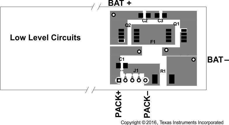
A battery fuel gauge circuit board is a challenging environment due to the fundamental incompatibility of high-current traces and ultra-low current semiconductor devices. The best way to protect against unwanted trace-to-trace coupling is with a component placement, such as that shown in Figure 11-1, where the high-current section is on the opposite side of the board from the electronic devices. Clearly, this is not possible in many situations due to mechanical constraints. Still, every attempt should be made to route high-current traces away from signal traces, which enter the BQ40Z50-R2 directly. IC references and registers can be disturbed and in rare cases damaged due to magnetic and capacitive coupling from the high-current path.
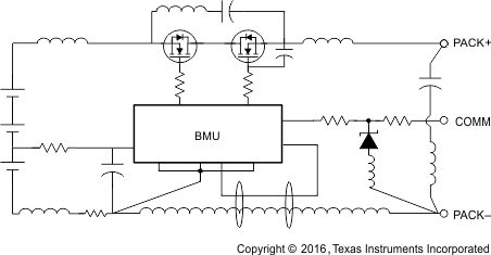
During surge current and ESD events, the high-current traces appear inductive and can couple unwanted noise into sensitive nodes of the gas gauge electronics, as illustrated in Figure 11-2.
 Figure 11-1 Separating High- and Low-Current Sections Provides an Advantage in Noise Immunity
 Figure 11-2 Avoid Close Spacing Between High-Current and Low-Level Signal Lines
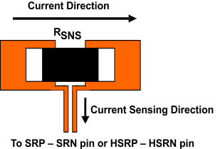
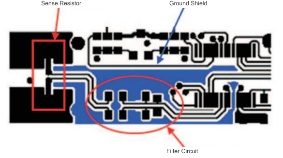
Kelvin voltage sensing is extremely important in order to accurately measure current and top and bottom cell voltages. Place all filter components as close as possible to the device. Route the traces from the sense resistor in parallel to the filter circuit. Adding a ground plane around the filter network can add additional noise immunity. Figure 11-3 and Figure 11-4 demonstrate correct Kelvin current sensing.
 Figure 11-3 Sensing Resistor PCB Layout
 Figure 11-4 Sense Resistor, Ground Shield, and Filter Circuit Layout