SLUSCS4C June 2017 – April 2021 BQ40Z50-R2
PRODUCTION DATA
- 1 Features
- 2 Applications
- 3 Description
- 4 Revision History
- 5 Description (continued)
- 6 Pin Configuration and Functions
-
7 Specifications
- 7.1 Absolute Maximum Ratings
- 7.2 ESD Ratings
- 7.3 Recommended Operating Conditions
- 7.4 Thermal Information
- 7.5 Supply Current
- 7.6 Power Supply Control
- 7.7 AFE Power-On Reset
- 7.8 AFE Watchdog Reset and Wake Timer
- 7.9 Current Wake Comparator
- 7.10 VC1, VC2, VC3, VC4, BAT, PACK
- 7.11 SMBD, SMBC
- 7.12 PRES, BTP_INT, DISP
- 7.13 LEDCNTLA, LEDCNTLB, LEDCNTLC
- 7.14 Coulomb Counter
- 7.15 CC Digital Filter
- 7.16 ADC
- 7.17 ADC Digital Filter
- 7.18 CHG, DSG FET Drive
- 7.19 PCHG FET Drive
- 7.20 FUSE Drive
- 7.21 Internal Temperature Sensor
- 7.22 TS1, TS2, TS3, TS4
- 7.23 PTC, PTCEN
- 7.24 Internal 1.8-V LDO
- 7.25 High-Frequency Oscillator
- 7.26 Low-Frequency Oscillator
- 7.27 Voltage Reference 1
- 7.28 Voltage Reference 2
- 7.29 Instruction Flash
- 7.30 Data Flash
- 7.31 OLD, SCC, SCD1, SCD2 Current Protection Thresholds
- 7.32 Timing Requirements: OLD, SCC, SCD1, SCD2 Current Protection Timing
- 7.33 Timing Requirements: SMBus
- 7.34 Timing Requirements: SMBus XL
- 7.35 Typical Characteristics
-
8 Detailed Description
- 8.1 Overview
- 8.2 Functional Block Diagram
- 8.3
Feature Description
- 8.3.1 Primary (1st Level) Safety Features
- 8.3.2 Secondary (2nd Level) Safety Features
- 8.3.3 Charge Control Features
- 8.3.4 Gas Gauging
- 8.3.5 Configuration
- 8.3.6 Battery Parameter Measurements
- 8.3.7 Battery Trip Point (BTP)
- 8.3.8 Lifetime Data Logging Features
- 8.3.9 Authentication
- 8.3.10 LED Display
- 8.3.11 IATA Support
- 8.3.12 Voltage
- 8.3.13 Current
- 8.3.14 Temperature
- 8.3.15 Communications
- 8.4 Device Functional Modes
- 9 Application and Implementation
- 10Power Supply Recommendations
- 11Layout
- 12Device and Documentation Support
- 13Mechanical, Packaging, and Orderable Information
Package Options
Mechanical Data (Package|Pins)
- RSM|32
Thermal pad, mechanical data (Package|Pins)
- RSM|32
Orderable Information
9.2.2.1.3 Li-Ion Cell Connections
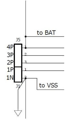
For cell connections, it is important to remember that high current flows through the top and bottom connections; therefore, the voltage sense leads at these points must be made with a Kelvin connection to avoid any errors due to a drop in the high-current copper trace. The location marked 4P in Figure 9-4 indicates the Kelvin connection of the most positive battery node. The connection marked 1N is equally important. The VC5 pin (a ground reference for cell voltage measurement), which is in the older generation devices, is not in the BQ40Z50-R2 device. Therefore, the single-point connection at 1N to the low-current ground is needed to avoid an unwanted voltage drop through long traces while the gas gauge is measuring the bottom cell voltage.
 Figure 9-4 Li-Ion Cell Connections