SLUSFB5 June 2024 BQ41Z50
ADVANCE INFORMATION
- 1
- 1 Features
- 2 Applications
- 3 Description
- 4 Description (continued)
- 5 Pin Configuration and Functions
-
6 Specifications
- 6.1 Absolute Maximum Ratings
- 6.2 ESD Ratings
- 6.3 Recommended Operating Conditions
- 6.4 Thermal Information
- 6.5 Supply Current
- 6.6 Power Supply Control
- 6.7 Current Wake Detector
- 6.8 VC0, VC1, VC2, VC3, VC4, PACK
- 6.9 SMBD, SMBC
- 6.10 PRES/SHUTDN, DISP
- 6.11 ALERT
- 6.12 Coulomb Counter Digital Filter (CC1)
- 6.13 ADC Digital Filter
- 6.14 CHG, DSG High-side NFET Drivers
- 6.15 Precharge (PCHG) FET Drive
- 6.16 FUSE Drive
- 6.17 Internal Temperature Sensor
- 6.18 TS1, TS2, TS3, TS4
- 6.19 Flash Memory
- 6.20 GPIO1, GPIO2, GPIO3, GPIO4, GPIO5, GPIO6, GPIO7
- 6.21 Elliptical Curve Cryptography (ECC)
- 6.22 SMBus Interface Timing
- 6.23 Typical Characteristics
-
7 Detailed Description
- 7.1 Overview
- 7.2 Functional Block Diagram
- 7.3 Feature Description
- 7.4 Device Functional Modes
- 8 Applications and Implementation
- 9 Device and Documentation Support
- 10Revision History
- 11Mechanical, Packaging, and Orderable Information
Package Options
Mechanical Data (Package|Pins)
- RSN|32
Thermal pad, mechanical data (Package|Pins)
Orderable Information
6.22 SMBus Interface Timing
Typical values stated where TA = 25°C and VBAT =
14.4V, Min/Max values stated where TA = –40°C to 85°C and
VBAT = 3.0V to 28V (unless otherwise noted)(1)
| PARAMETER | TEST CONDITIONS | MIN | TYP | MAX | UNIT | |
|---|---|---|---|---|---|---|
| SMBus 100kHz | ||||||
| fSMB | SMBus operating frequency | TARGET mode, SMBC 50% duty cycle | 10 | 100 | kHz | |
| fMAS | SMBus host clock frequency | 10 | 100 | kHz | ||
| tBUF | Bus free time between start and stop | 4.7 | µs | |||
| tHD:START | Hold time after (repeated) start | 4 | µs | |||
| tSU:START | Repeated start setup time | 4.7 | µs | |||
| tSU:STOP | Stop setup time | 4 | µs | |||
| tHD:DATA | Data hold time | 0 | ns | |||
| tSU:DATA | Data setup time | 250 | ns | |||
| tTIMEOUT | Error signal detect time | 25 | 35 | ms | ||
| tLOW | Clock low period | 4.7 | µs | |||
| tHIGH | Clock high period | 4 | 50 | µs | ||
| tLOW(SEXT) | Cumulative clock low target extend time | 25 | ms | |||
| tLOW(MEXT) | Cumulative clock low host extend time | 10 | ms | |||
| tF | Clock fall time | VIH(MIN) + 0.15 to VIL(MAX) – 0.15 | 300 | ns | ||
| tR | Clock rise time | VIL(MAX) – 0.15 to VIH(MIN) + 0.15 | 1000 | ns | ||
| tBUSLO | Max SMBC/SMBD Low (BUSLO) Signal Detect Time by device | BLTx = 0x1 to 0x7 | 0.5 | 3.5 | s | |
| ΔtBUSLO | BUSLO detect time program step | 0.5 | s | |||
| CD | Capacitive load for each bus line | 400 | pF | |||
| SMBus 400kHz | ||||||
| fSMB | SMBus operating frequency | TARGET mode, SMBC 50% duty cycle | 10 | 400 | kHz | |
| fMAS | SMBus host clock frequency | 10 | 400 | kHz | ||
| tBUF | Bus free time between start and stop | 1.3 | µs | |||
| tHD:START | Hold time after (repeated) start | 0.6 | µs | |||
| tSU:START | Repeated start setup time | 0.6 | µs | |||
| tSU:STOP | Stop setup time | 0.6 | µs | |||
| tHD:DATA | Data hold time | 0 | ns | |||
| tSU:DATA | Data setup time | 100 | ns | |||
| tTIMEOUT | Error signal detect time | 25 | 35 | ms | ||
| tLOW | Clock low period | 1.3 | µs | |||
| tHIGH | Clock high period | 0.6 | 50 | µs | ||
| tLOW(SEXT) | Cumulative clock low target extend time | 25 | ms | |||
| tLOW(MEXT) | Cumulative clock low host extend time | 10 | ms | |||
| tF | Clock fall time | VIH(MIN) + 0.15 to VIL(MAX) – 0.15 | 300 | ns | ||
| tR | Clock rise time | VIL(MAX) – 0.15 to VIH(MIN) + 0.15 | 300 | ns | ||
| tBUSLO | Max SMBC/SMBD Low (BUSLO) Signal Detect Time by device | BLTx = 0x1 to 0x7 | 0.5 | 3.5 | s | |
| ΔtBUSLO | BUSLO detect time program step | 0.5 | s | |||
| CD | Capacitive load for each bus line | 400 | pF | |||
| SMBus 1MHz | ||||||
| fSMB | SMBus operating frequency | TARGET mode, SMBC 50% duty cycle | 10 | 1000 | kHz | |
| fMAS | SMBus host clock frequency | 10 | 1000 | kHz | ||
| tBUF | Bus free time between start and stop | 0.5 | µs | |||
| tHD:START | Hold time after (repeated) start | 0.26 | µs | |||
| tSU:START | Repeated start setup time | 0.26 | µs | |||
| tSU:STOP | Stop setup time | 0.26 | µs | |||
| tHD:DATA | Data hold time | 0 | ns | |||
| tSU:DATA | Data setup time | 50 | ns | |||
| tTIMEOUT | Error signal detect time | 25 | 35 | ms | ||
| tLOW | Clock low period | 0.5 | µs | |||
| tHIGH | Clock high period | 0.26 | 50 | µs | ||
| tLOW(SEXT) | Cumulative clock low target extend time | 25 | ms | |||
| tLOW(MEXT) | Cumulative clock low host extend time | 10 | ms | |||
| tF | Clock fall time | VIH(MIN) + 0.15 to VIL(MAX) – 0.15 | 120 | ns | ||
| tR | Clock rise time | VIL(MAX) – 0.15 to VIH(MIN) + 0.15 | 120 | ns | ||
| tBUSLO | Max SMBC/SMBD Low (BUSLO) Signal Detect Time by device | BLTx = 0x1 to 0x7 | 0.5 | 3.5 | s | |
| ΔtBUSLO | BUSLO detect time program step | 0.5 | s | |||
| CD | Capacitive load for each bus line | 100 | pF | |||
(1) Specified by design. Not
production tested
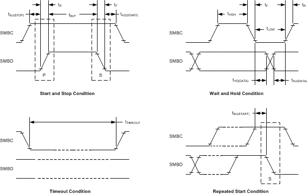
 Figure 6-1 SMBus Timing Diagram
 Figure 6-1 SMBus Timing Diagram