SLUSCP1A August 2016 – August 2016
PRODUCTION DATA.
- 1 Features
- 2 Applications
- 3 Description
- 4 Revision History
- 5 Pin Configuration and Functions
- 6 Specifications
- 7 Detailed Description
- 8 Application and Implementation
- 9 Power Supply Recommendations
- 10Layout
- 11Device and Documentation Support
- 12Mechanical, Packaging, and Orderable Information
Package Options
Mechanical Data (Package|Pins)
- RHB|32
Thermal pad, mechanical data (Package|Pins)
- RHB|32
Orderable Information
10 Layout
10.1 Layout Guidelines
Careful PCB layout practice is critical to proper system operation. Many references are available on proper PCB layout techniques. A few good tips are as follows.
The TX layout requires a 4-layer PCB layout for best ground plane technique. A 2-layer PCB layout can be achieved though not as easily. Ideally, the approach to the layer stack-up is:
- Layer 1 component placement and as much ground plane as possible
- Layer 2 clean ground
- Layer 3 finish routing
- Layer 4 clean ground
Thus, the circuitry is virtually sandwiched between grounds. This minimizes EMI noise emissions and also provides a noise-free voltage reference plane for device operation.
Keep as much copper as possible. Make sure the bq500511A GND pins have a continuous flood connection to the ground plane. The power pad of the bq50002A should also be stitched to the ground plane, which also acts as a heat sink. A good GND reference is necessary for proper system operation, such as analog-digital conversion, clock stability, and best overall EMI performance. Separate the analog ground plane from the power ground plane and use only one tie point to connect grounds. Having several tie points defeats the purpose of separating the grounds. See the bq50002 EVM, SLVUAJ7, for an example of a good layout technique.
10.1.1 Layout Notes
Make sure the bypass capacitors intended for the bq500511A 3.3-V supply are actually bypassing these supply pins (pin 32, DVCC, and pin 40, AVCC) to solid ground plane (see Figure 11). This means they need to be placed as close to the device as possible and the traces must be as wide as possible.
Make sure the bq500511A has a continuous flood connection to the ground plane (see Figure 12).
The full-bridge power stage that drives the TX coil is composed of two half-bridge power stages (integrated in bq50002A) and resonant capacitors. Inputs bypass capacitors should be placed as close as possible to the bq50002A PVIN1 pins (pin 27, 28) and PVIN2 pins (pin 14, 15). The input and ground pours and traces should be made as wide as possible for better current flow. The trace to the coil and resonant capacitors should also be made as wide as possible (see Figure 13).
To ensure proper operation, grounds conducting a large amount of current and switching noise must be isolated from low current, quiet grounds. Separate the ground pours for the power stages and the bq500511A IC. Connect all grounds to a single point at the main ground terminal (see Figure 13).
Proper current sensing layout technique is very important, as it directly affects the FOD and PMOD performance. When sampling the very-low voltages generated across a current sense resistor, be sure to use the so called 4- wire or Kelvin-connection technique. This is important to avoid introducing false voltage drops from adjacent pads and copper power routes. It is a common power-supply layout technique. Some high-accuracy sense resistors have dedicated sense pins (see Figure 15).
The trace from bq50002A CSP pin to sense resistor must be minimized to avoid unwanted offset in the application. This trace should be limited to less than 20 mΩ resistance.
10.2 Layout Examples
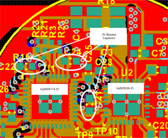 Figure 11. Bypass Capacitors Layout
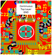 Figure 12. Continuous GND Layout
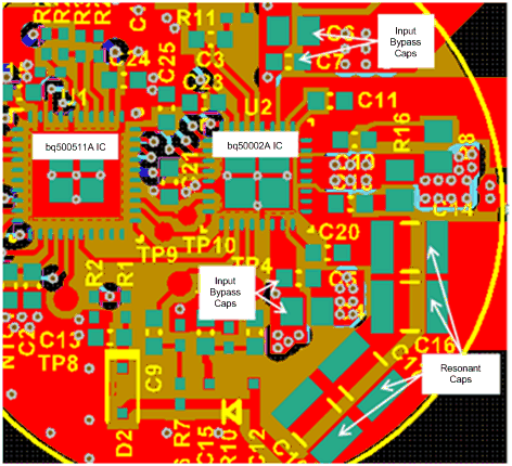 Figure 13. Ground Layout
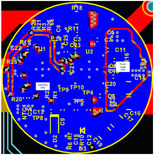 Figure 14. Ground Layout
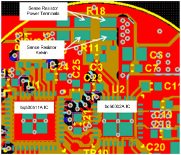 Figure 15. Current Sensing Layout