SLUSB42F July 2012 – June 2017
PRODUCTION DATA.
- 1 Features
- 2 Applications
- 3 Description
- 4 Revision History
- 5 Device Options
- 6 Pin Configuration and Functions
- 7 Specifications
-
8 Detailed Description
- 8.1 Overview
- 8.2 Functional Block Diagram
- 8.3
Feature Description
- 8.3.1 Using the bq5105x as a Wireless Li-Ion/Li-Pol Battery Charger (With Reference to )
- 8.3.2 Details of a Qi Wireless Power System and bq5105xB Power Transfer Flow Diagrams
- 8.3.3 Battery Charge Profile
- 8.3.4
Battery Charging Process
- 8.3.4.1 Precharge Mode (VBAT ≤ VLOWV)
- 8.3.4.2 Fast Charge Mode / Constant Voltage Mode
- 8.3.4.3 Battery Charge Current Setting Calculations
- 8.3.4.4 Battery-Charger Safety and JEITA Guidelines
- 8.3.4.5 Input Overvoltage
- 8.3.4.6 End Power Transfer Packet (WPC Header 0x02)
- 8.3.4.7 Status Output
- 8.3.4.8 Communication Modulator
- 8.3.4.9 Adaptive Communication Limit
- 8.3.4.10 Synchronous Rectification
- 8.3.4.11 Internal Temperature Sense (TS Function of the TS/CTRL Pin)
- 8.3.4.12 WPC v1.2 Compatibility
- 8.4 Device Functional Modes
- 9 Application and Implementation
- 10Power Supply Recommendations
- 11Layout
- 12Device and Documentation Support
- 13Mechanical, Packaging, and Orderable Information
Package Options
Refer to the PDF data sheet for device specific package drawings
Mechanical Data (Package|Pins)
- RHL|20
- YFP|28
Thermal pad, mechanical data (Package|Pins)
- RHL|20
Orderable Information
8 Detailed Description
8.1 Overview
8.1.1 A Brief Description of the Wireless System
A wireless system consists of a charging pad (primary, transmitter) and the secondary-side equipment. There are coils in the charging pad and in the secondary equipment which magnetically couple to each other when the equipment is placed on the charging pad. Power is transferred from the primary to the secondary by transformer action between the coils. Control over the amount of power transferred is achieved by changing the frequency of the primary drive.
The secondary can communicate with the primary by changing the load seen by the primary. This load variation results in a change in the primary coil current, which is measured and interpreted by a processor in the charging pad. The communication is digital - packets are transferred from the secondary to the primary. Differential bi-phase encoding is used for the packets. The rate is 2-kbps.
Various types of communication packets have been defined. These include identification and authentication packets, error packets, control packets, power usage packets, end of power packet and efficiency packets.
The primary coil is powered off most of the time. It wakes up occasionally to see if a secondary is present. If a secondary authenticates itself to the primary, the primary remains powered up. The secondary maintains full control over the power transfer using communication packets.
 Figure 19. WPC Wireless Power Charging System Indicating the Functional Integration of the bq5105x
8.2 Functional Block Diagram
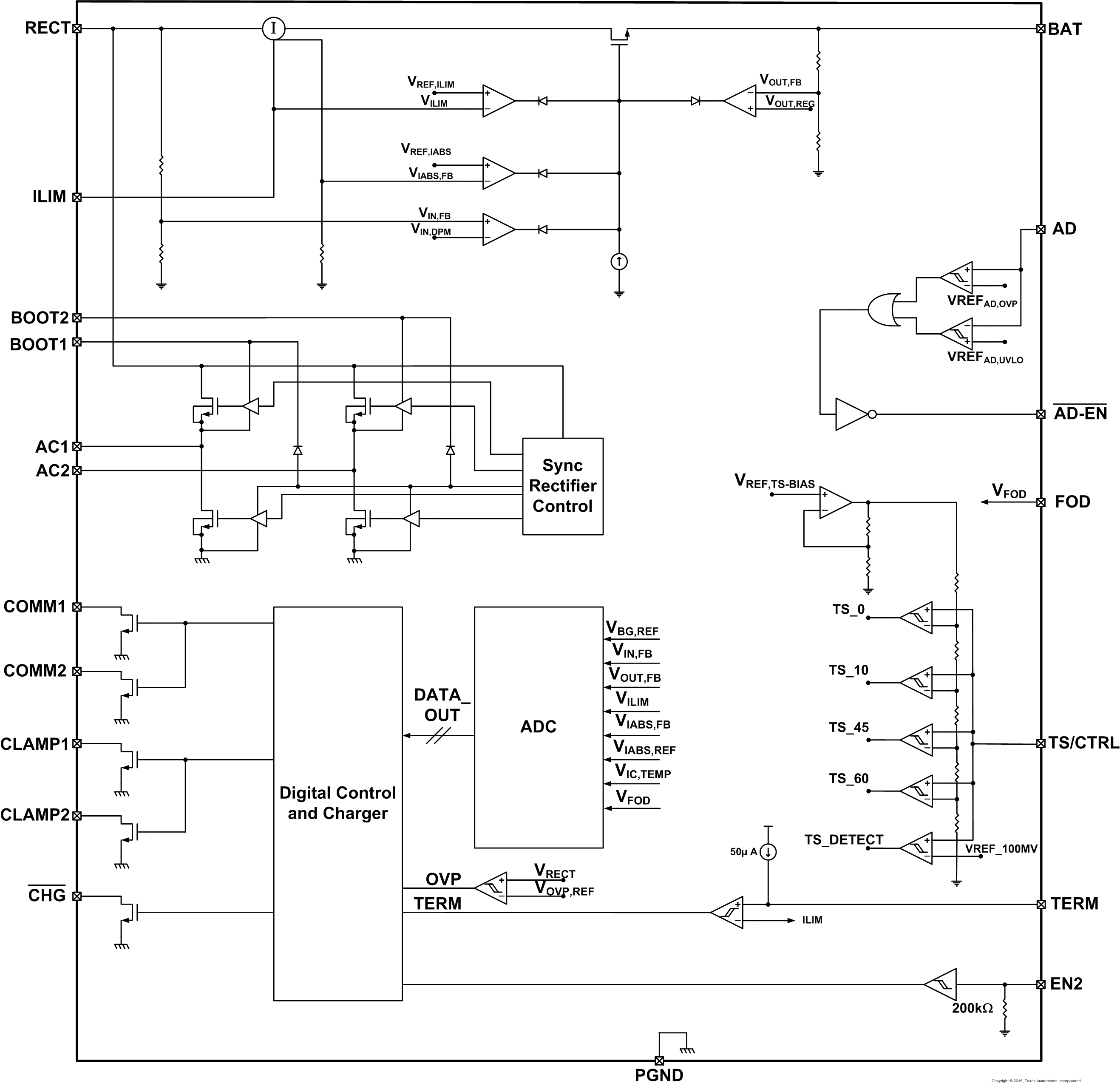
8.3 Feature Description
8.3.1 Using the bq5105x as a Wireless Li-Ion/Li-Pol Battery Charger (With Reference to Functional Block Diagram)
Functional Block Diagram is the schematic of a system which uses the bq5105x as a direct battery charger. When the system shown in Functional Block Diagram is placed on the charging pad (transmitter), the receiver coil couples to the magnetic flux generated by the coil in the charging pad which consequently induces a voltage in the receiver coil. The internal synchronous rectifier feeds this voltage to the RECT pin which has the filter capacitor C3.
The bq5105x identifies and authenticates itself to the primary using the COMM pins by switching on and off the COMM FETs and hence switching in and out CCOMM. If the authentication is successful, the transmitter will remain powered on. The bq5105x measures the voltage at the RECT pin, calculates the difference between the actual voltage and the desired voltage VRECT-REG and sends back error packets to the primary. This process goes on until the RECT voltage settles at VRECT-REG.
During power-up, the LDO is held off until the VRECT-REG threshold converges. The voltage control loop ensures that the output (BAT) voltage is maintained at VBAT-REG. The values of VBAT and VRECT are dependant on the battery charge mode. The bq5105x continues to monitor the VRECT and VBAT and sends error packets to the primary every 250 ms. The bq5105x regulates the VRECT voltage very close to battery voltage, this voltage tracking process minimizes the voltage difference across the internal LDO and maximizes the charging efficiency. If a large transient occurs, the feedback to the primary speeds up to every 32 ms in order to converge on an operating point in less time.
8.3.2 Details of a Qi Wireless Power System and bq5105xB Power Transfer Flow Diagrams
The bq5105xB integrates a fully compliant WPC v1.2 communication algorithm in order to streamline receiver designs (no extra software development required). Other unique algorithms such as Dynamic Rectifier Control are also integrated to provide best-in-class system performance. This section provides a high level overview of these features by illustrating the wireless power transfer flow diagram from start-up to active operation.
During start-up operation, the wireless power receiver must comply with proper handshaking to be granted a power contract from the TX. The TX will initiate the handshake by providing an extended digital ping. If an RX is present on the TX surface, the RX will then provide the signal strength, configuration and identification packets to the TX (see volume 1 of the WPC specification for details on each packet). These are the first three packets sent to the TX. The only exception is if there is a shutdown condition on the EN1/EN2, AD, or TS/CTRL pins where the Rx will shut down the TX immediately. Once the TX has successfully received the signal strength, configuration and identification packets, the RX will be granted a power contract and is then allowed to control the operating point of the power transfer. With the use of the bq5105xB Dynamic Rectifier Control algorithm, the RX will inform the TX to adjust the rectifier voltage above 5 V before enabling the output supply. This method enhances the transient performance during system start-up. See Figure 20 for the start-up flow diagram details.
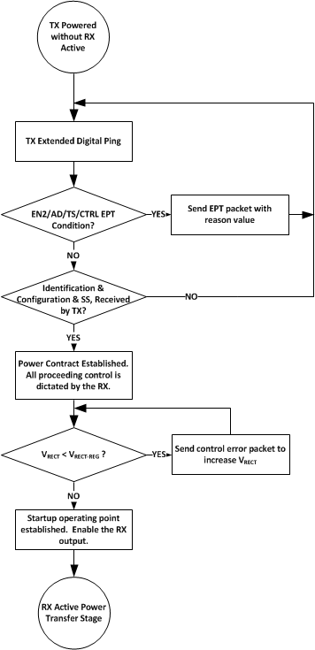 Figure 20. Wireless Power Start-up Flow Diagram
Once the start-up procedure has been established, the RX will enter the active power transfer stage. This is considered the “main loop” of operation. The Dynamic Rectifier Control algorithm will determine the rectifier voltage target based on a percentage of the maximum output current level setting (set by KILIM and the IILIM resistance to PGND). The RX will send control error packets in order to converge on these targets. As the output current changes, the rectifier voltage target will dynamically change. As a note, the feedback loop of the WPC system is relatively slow where it can take up to 90 ms to converge on a new rectifier voltage target. It should be understood that the instantaneous transient response of the system is open loop and dependent on the RX coil output impedance at that operating point. More details on this will be covered in the section Receiver Coil Load- Line Analysis. The “main loop” will also determine if any conditions are true and will then discontinue the power transfer. Figure 21 shows the active power transfer loop.
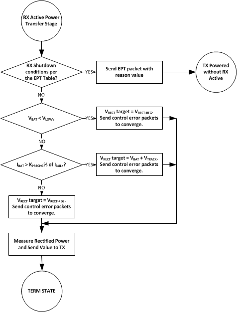 Figure 21. Active Power Transfer Flow Diagram
 Figure 22. TERM STATE Flow Diagram of bq5105XB
8.3.3 Battery Charge Profile
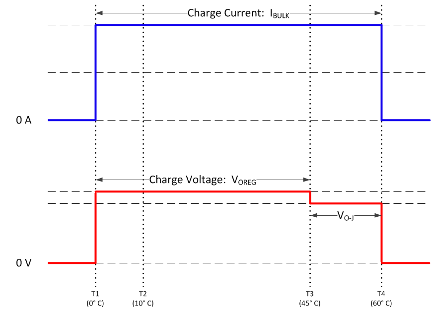
The battery is charged in three phases: precharge, fast-charge constant current and constant voltage. A voltage-based battery pack thermistor monitoring input (TS function of the TS/CTRL pin) is included that monitors battery temperature for safe charging. The TS function for bq51050B and bq51051B is JEITA compatible. The TS function for the bq51052B modifies the current regulation differently than standard JEITA. See Battery-Charger Safety and JEITA Guidelines for more details.
The rectifier voltage follows BAT voltage plus VTRACK for any battery voltage above VLOWV to full regulation voltage and most of the taper charging phase. If the battery voltage is below VLOWV the rectifier voltage increases to VRECT-REG.
If IBAT is less than IEndTrack (a percentage of IBULK) during taper mode, the rectifier voltage increases to VRECT-REG.
The charge profile for the bq51050B and bq51051B is shown in Figure 23 while the bq51052B is shown in Figure 24.
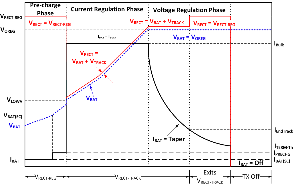 Figure 23. bq51050B and bq51051B Li-Ion Battery Charge Profile
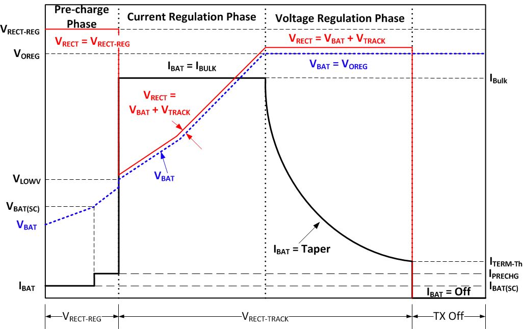 Figure 24. bq51052B Li-Ion Battery Charge Profile
8.3.4 Battery Charging Process
8.3.4.1 Precharge Mode (VBAT ≤ VLOWV)
The bq5105X enters precharge mode when VBAT ≤ VLOWV. Upon entering precharge mode, battery charge current limit is set to IPRECHG. During precharge mode, the charge current is regulated to KPRECHG percent of the fast charge current (IBULK) setting. For example, if IBULK is set to 800 mA, then the precharge current would have a typical value of 160 mA.
If the battery is deeply discharged or shorted (VBAT < VBAT(SC)), the bq5105X applies IBAT(SC) current to bring the battery voltage up to acceptable charging levels. Once the battery rises above VBAT(SC), the charge current is regulated to IPRECHG.
Under normal conditions, the time spent in this precharge region is a very short percentage of the total charging time and this does not affect the overall charging efficiency for very long.
8.3.4.2 Fast Charge Mode / Constant Voltage Mode
Once VBAT > VLOWV, the bq5105x enters fast charge mode (Current Regulation Phase) where charge current is regulated using the internal MOSFETs between RECT and BAT. Once the battery voltage charges up to VBAT-REG, the bq5105x enters constant voltage (CV) phase and regulates battery voltage to VOREG and the charging current is reduced.
Once IBAT falls below the termination threshold (ITERM-Th), the charger sends an EPT (Charge Complete) notification to the TX and enters high impedance mode.
8.3.4.3 Battery Charge Current Setting Calculations
8.3.4.3.1 RILIM Calculations
The bq5105x includes a means of providing hardware overcurrent protection by means of an analog current regulation loop. The hardware current limit provides an extra level of safety by clamping the maximum allowable output current (for example, a current compliance). The calculation for the total RILIM resistance is as follows:

Where IBULK is the programmed battery charge current during fast charge mode. When referring to the application diagram shown in Figure 32, RILIM is the sum of RFOD and R1 (the total resistance from the ILIM pin to PGND).
8.3.4.3.2 Termination Calculations
The bq5105X includes a programmable upper termination threshold. The upper termination threshold is calculated using Equation 2:

The KTERM constant is specified in Electrical Characteristics as 240 Ω/%. The upper termination threshold is set as a percentage of the charge current setting (IBULK).
For example, if RILIM is set to 314 Ω, IBULK will be 1 A (314 ÷ 314). If the upper termination threshold is desired to be 100 mA, this would be 10% of IBULK. The RTERM resistor would then equal 2.4 kΩ (240 × 10).
Termination can be disabled by floating the TERM pin. If the TERM pin is grounded the termination function is effectively disabled. However, due to offsets of internal comparators, termination may occur at low battery currents.
8.3.4.4 Battery-Charger Safety and JEITA Guidelines
The bq5105x continuously monitors battery temperature by measuring the voltage between the TS/CTRL pin and PGND. A negative temperature coefficient thermistor (NTC) and an external voltage divider typically develop this voltage. The bq5105x compares this voltage against its internal thresholds to determine if charging is allowed. To initiate a charge cycle, the voltage on TS/CTRL pin (VTS) must be within the VT1 to VT4 thresholds. If VTS is outside of this range, the bq5105x suspends charge and waits until the battery temperature is within the VT1 to VT4 range. Additional information on the Temperature Sense function can be found in Internal Temperature Sense (TS Function of the TS/CTRL Pin).
8.3.4.4.1 bq51050B and bq51051B JEITA
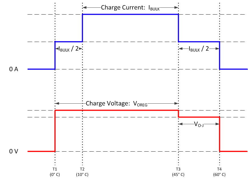
If VTS is within the ranges of VT1 and VT2 or VT3 and VT4, the charge current is reduced to IBULK/2. If VTS is within the range of VT1 and VT3, the maximum charge voltage regulation is VOREG. If VTS is within the range of VT3 and VT4, the maximum charge voltage regulation is reduced to "NEW SPEC". Figure 25 summarizes the operation.
8.3.4.5 Input Overvoltage
If, for some condition (for example, a change in position of the equipment on the charging pad), the rectifier voltage suddenly increases in potential, the voltage-control loop inside the bq5105x becomes active, and prevents the output from going beyond VBAT-REG. The receiver then starts sending back error packets every 32 ms until the RECT voltage comes back to an acceptable level, and then maintains the error communication every 250 ms.
If the input voltage increases in potential beyond VOVP, the device switches off the internal FET and communicates to the primary to bring the voltage back to VRECT-REG. In addition a proprietary voltage protection circuit is activated by means of CCLAMP1 and CCLAMP2 that protects the device from voltages beyond the maximum rating.
8.3.4.6 End Power Transfer Packet (WPC Header 0x02)
The WPC allows for a special command to terminate power transfer from the TX termed End Power Transfer (EPT) packet. WPC v1.2 specifies the reasons for sending a termination packet and their data field value. In Table 1, the CONDITION column corresponds to the stimulus causing the bq5105x device to send the hexidecimal code in the VALUE column.
Table 1. Termination Packets
8.3.4.7 Status Output
The bq5105x provides one status output, CHG. This output is an open-drain NMOS device that is rated to 20 V. The open-drain FET connected to the CHG pin will be turned on whenever the output (BAT) of the charger is enabled. As a note, the output of the charger supply will not be enabled if the VRECT-REG does not converge to the no-load target voltage.
8.3.4.8 Communication Modulator
The bq5105x provides two identical, integrated communication FETs which are connected to the pins COMM1 and COMM2. These FETs are used for modulating the secondary load current which allows bq5105x to communicate error control and configuration information to the transmitter.There are two methods to implement load modulation, capacitive and resistive.
Capacitive load modulation is more commonly used. Capacitive load modulation is shown in Figure 27. In this case, a capacitor is connected from COMM1 to AC1 and from COMM2 to AC2. When the COMM switches are closed there is effectively a 22 nF capacitor connected between AC1 and AC2. Connecting a capacitor in between AC1 and AC2 modulates the impedance seen by the coil, which will be reflected to the primary and interpreted by the controller as a change in current.
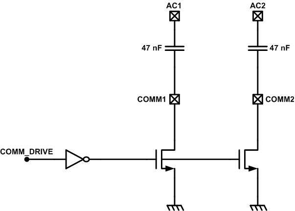 Figure 27. Capacitive Load Modulation
Figure 28 shows how the COMM pins can be used for resistive load modulation. Each COMM pin can handle at most a 24 Ω communication resistor. Therefore, if a COMM resistor between 12 Ω and 24 Ω is required, COMM1 and COMM2 pins must be connected in parallel. bq5105x does not support a COMM resistor less than 12 Ω.
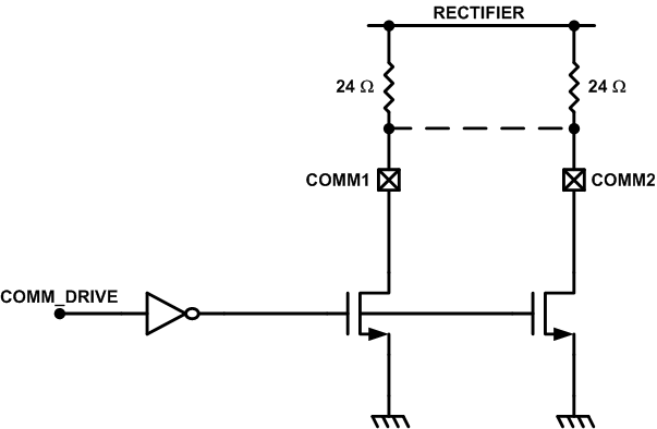 Figure 28. Resistive Load Modulation
8.3.4.9 Adaptive Communication Limit
The Qi communication channel is established through backscatter modulation as described in the previous sections. This type of modulation takes advantage of the loosely coupled inductor relationship between the RX and TX coils. Essentially, the switching in-and-out of the communication capacitor or resistor adds a transient load to the RX coil in order to modulate the TX coil voltage and current waveform (amplitude modulation). The consequence of this technique is that a load transient (load current noise) from the mobile device has the same signature. To provide noise immunity to the communication channel, the output load transients must be isolated from the RX coil. The proprietary feature Adaptive Communication Limit achieves this by dynamically adjusting the current limit of the regulator.
This can be seen in Figure 12. In this plot, an output load is limited to 400 mA during communications time. The pulses on VRECT indicate that a communication packet event is occurring. The regulator limits the load to a constant 400 mA and, therefore, preserves communication.
8.3.4.10 Synchronous Rectification
The bq5105x provides an integrated, self-driven synchronous rectifier that enables high-efficiency AC to DC power conversion. The rectifier consists of an all NMOS H-Bridge driver where the back gates of the diodes are configured to be the rectifier when the synchronous rectifier is disabled. During the initial start-up of the WPC system the synchronous rectifier is not enabled. At this operating point, the DC rectifier voltage is provided by the diode rectifier. Once VRECT is greater than VUVLO, half synchronous mode will be enabled until the load current surpasses IBAT-SR. Above IBAT-SR the full synchronous rectifier stays enabled until the load current drops back below the hysteresis level (IBAT-SRH) where half synchronous mode is re-enabled.
8.3.4.11 Internal Temperature Sense (TS Function of the TS/CTRL Pin)
The bq5105x includes a ratiometric battery temperature sense circuit. The temperature sense circuit has two ratiometric thresholds which represent hot and cold conditions. An external temperature sensor is recommended to provide safe operating conditions to the receiver product. This pin is best used when monitoring the battery temperature.
The circuits in Figure 29 allow for any NTC resistor to be used with the given VHOT and VCOLD thresholds. The thermister characteristics and threshold temperatures selected will determine which circuit is best for an application.
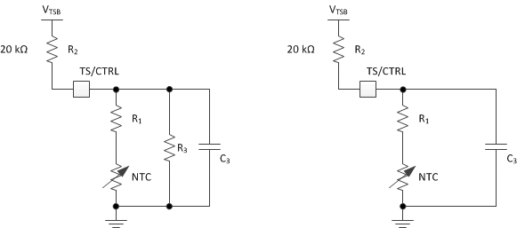 Figure 29. NTC Circuit Options for Safe Operation of the Wireless Receiver Power Supply
The resistors R1 and R3 can be solved by resolving the system of equations at the desired temperature thresholds. The two equations are:

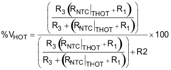
Where:
TCOLD and THOT are the desired temperature thresholds in degrees Kelvin. Ro is the nominal resistance at T0 (25°C) and β is the temperature coefficient of the NTC resistor. For an example solution for part number ERT-JZEG103JA see the BQ5105XB NTC Calculator Tool, (SLUS629).
Where,
TCOLD = 0°C (273.15°K)
THOT = 60°C (333.15°K)
β = 3380
Ro = 10 kΩ
The plot of the percent VTSB versus temperature is shown in Figure 30:
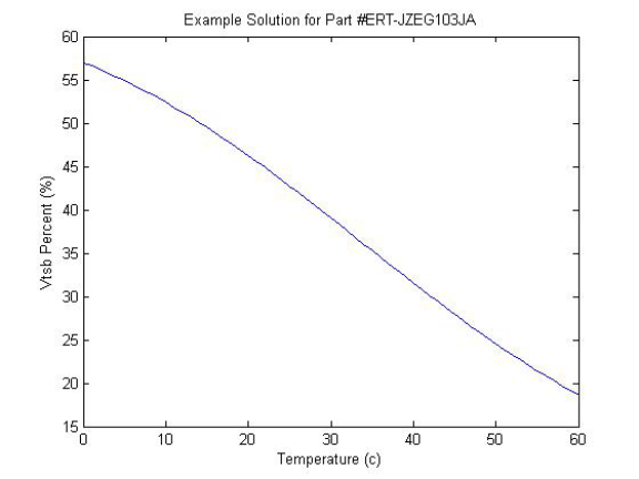 Figure 30. Example Solution for Panasonic Part # ERT-JZEG103JA
Figure 31 shows the periodic biasing scheme used for measuring the TS state. An internal TS_READ signal enables the TS bias voltage for 25 ms. During this period the TS comparators are read (each comparator has a 10-ms deglitch) and appropriate action is taken based on the temperature measurement. After this 25-ms period has elapsed the TS_READ signal goes low, which causes the TS/CTRL pin to become high impedance. During the next 100-ms period, the TS voltage is monitored and compared to VCTRL-HI. If the TS voltage is greater than VCTRL-HI then a secondary device is driving the TS/CTRL pin and a CTRL = 1 is detected.
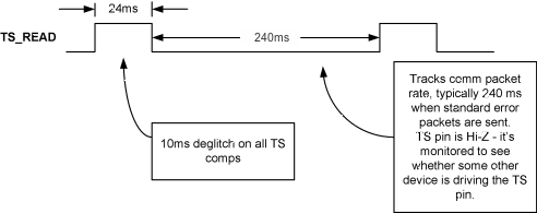 Figure 31. Timing Diagram for TS Detection Circuit
8.3.4.11.1 TS/CTRL Function
The TS/CTRL pin offers three functions:
- NTC temperature monitoring
- Charge done indication
- Fault indication
When an NTC resistor is connected between the TS/CTRL pin and PGND, the NTC function is allowed to operate. This functionality can effectively be disabled by connecting a 10 kΩ resistor from TS/CRTL to PGND. If the TS/CTRL pin is pulled above VCTRL-HI, the RX is shut down with the indication of a charge complete condition. If the TS/CTRL pin is pulled below VCTRL-LOW, the RX is shut down with the indication of a fault.
8.3.4.11.2 Thermal Protection
The bq5105x includes thermal shutdown protection. If the die temperature reaches TJ-SD, the LDO is shut off to prevent any further power dissipation. Once the temperature falls TJ-Hys below TJ-SD, operation can continue.
8.3.4.12 WPC v1.2 Compatibility
The bq5105x is a WPC v1.2 compatible device. In order to enable a Power Transmitter to monitor the power loss across the interface as one of the possible methods to limit the temperature rise of Foreign Objects, the bq5105x reports its Received Power to the Power Transmitter. The Received Power equals the power that is available from the output of the Power Receiver plus any power that is lost in producing that output power. For example, the power loss includes (but is not limited to) the power loss in the Secondary Coil and series resonant capacitor, the power loss in the Shielding of the Power Receiver, the power loss in the rectifier, the power loss in any post-regulation stage, and the eddy current loss in metal components or contacts within the Power Receiver. In the WPC v1.2 specification, foreign object detection (FOD) is enforced, that means the bq5105x will send received power information with known accuracy to the transmitter.
WPC v1.2 defines Received Power as “the average amount of power that the Power Receiver receives through its Interface Surface, in the time window indicated in the Configuration Packet”.
A Receiver will be certified as WPC v1.2 only after meeting the following requirement. The device under test (DUT) is tested on a Reference Transmitter whose transmitted power is calibrated, the receiver must send a received power such that:
This 250 mW bias ensures that system will remain interoperable.
WPC v1.2 Transmitters will be tested to see if they can detect reference Foreign Objects with a Reference receiver. The WPC v1.2 specification allows much more accurate sensing of Foreign Objects than WPC v1.0.
A Transmitter can be certified as a WPC v1.2 only after meeting the following requirement. A Transmitter is tested to see if it can prevent some reference Foreign Objects (disc, coin, foil) from exceeding their threshold temperature (60°C, 80°C).
8.4 Device Functional Modes
The general modes of battery charging are described above in the Feature Description. The bq5105x devices have several functional modes. Start-up refers to the initial power transfer and communication between the receiver (bq5105x circuit) and the transmitter. Power transfer refers to any time that the TX and RX are communicating and power is being delivered from the TX to the RX. Charge termination covers intentional termination (charge complete) and unintentional termination (removal of the RX from the TX, over temperature or other fault conditions).
